Chapter: Digital Logic Circuits : Synchronous Sequential Circuits
D Flip Flop
D Flip-Flop
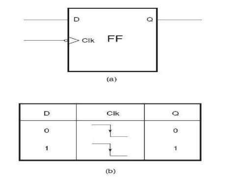
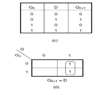
A D flip-flop, also called a delay flip-flop, can be used to provide temporary storage of one bit of information. Figure shows the circuit symbol and function table of a negative edge-triggered D flip-flop. When the clock is active, the data bit (0 or 1) present at the D input is transferred to the output. In the D flip-flop of Fig the data transfer from D input to Q output occurs on the negative-going (HIGH-to-LOW) transition of the clock input. The D input can acquire new status


D Type Flip Flop
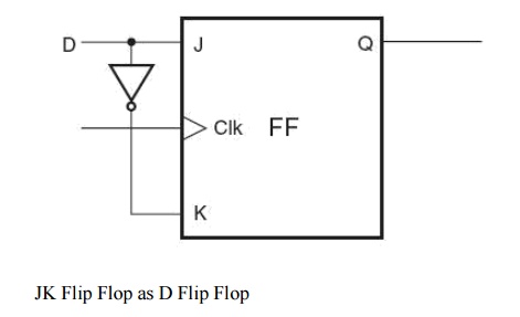
J-K Flip-Flop as D Flip-Flop
Figure below shows how a J-K flip-flop can be used as a D flip-flop. When the D input is a logic ‘1‘, the J and K inputs are a logic ‘1‘ and ‘0‘respectively. According to the function table of the J-K flip-flop, under these input conditions, the Q output will go to the logic ‘1‘ state when clocked. Also, when the D input is a logic ‘0‘, the J and K inputs are a logic ‘0‘ and ‘1‘ respectively. Again, according to the function table of the J-K flip-flop, under these input conditions, the Q output will go to the logic ‘0‘ state when clocked. Thus, in both cases, the D input is passed on to the output when the flip-flop is clocked.

Related Topics