Chapter: Digital Logic Circuits : VHDL
Clocked sequential system
Clocked sequential system
In digital electronics, a clocked sequential system is a system whose output depends only on the current state, whose state changes only when a global clock signal changes, and whose next-state depends only on the current state and the inputs.
Nearly all digital electronic devices (microprocessors, digital clocks, mobile phones, cordless telephones, electronic calculators, etc.) are designed as clocked sequential systems. Notable exceptions include digital asynchronous logic systems.
In particular, nearly all computers are designed as clocked sequential systems. Notable exceptions include analog computers and clockless CPUs.
Typically each bit of the "state" is contained in its own flip-flop. Combinational logic decodes the state into the output signals. More combinational logic encodes the current state and the inputs into the next-state signals. The next-state signals are latched into the flipflops under the control of the global clock signal (a wire connected to every flip-flop).
A clocked sequential system is a kind of Moore machine.
Adder
In electronics, an adder or summer is a digital circuit that performs addition of numbers. In modern computers adders reside in the arithmetic logic unit (ALU) where other operations are performed. Although adders can be constructed for many numerical representations, such as Binary-coded decimal or excess-3, the most common adders operate on binary numbers. In cases where two's complement or one's complement is being used to represent negative numbers, it is trivial to modify an adder into an adder-subtractor. Other signed number representations require a more complex adder.
Half adder
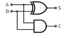
Example half adder circuit diagram
A half adder adds two one-bit binary numbers A and B. It has two outputs, S and C (the value theoretically carried on to the next addition); the final sum is 2C + S. The simplest half-adder design, pictured on the right, incorporates an XOR gate for S and an AND gate for C. Half adders cannot be used compositely, given their incapacity for a carry-in bit.
Full adder
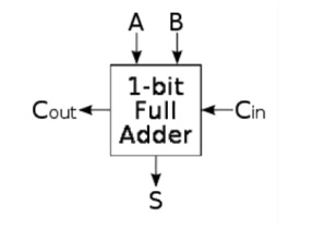
Schematic symbol for a 1-bit full adder with Cin and Cout drawn on sides of block to emphasize their use in a multi-bit adder
A full adder adds binary numbers and accounts for values carried in as well as out. A one-bit full adder adds three one-bit numbers, often written as A, B, and Cin; A and B are the operands, and Cin is a bit carried in (in theory from a past addition). The circuit produces a
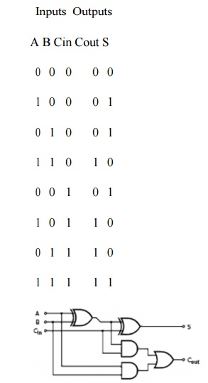
Example full adder circuit diagram; the AND and OR gates can be replaced with NAND gates for the same results
A full adder can be implemented in many different ways such as with a custom transistor-level circuit or composed of other gates. One example implementation is with

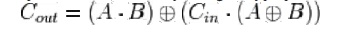
In this implementation, the final OR gate before the carry-out output may be replaced by an XOR gate without altering the resulting logic. Using only two types of gates is convenient if the circuit is being implemented using simple IC chips which contain only one gate type per chip. In this light, Cout can be implemented as
A full adder can be constructed from two half adders by connecting A and B to the input of one half adder, connecting the sum from that to an input to the second adder, connecting Ci to the other input and OR the two carry outputs. Equivalently, S could be made the three-bit XOR of A, B, and Ci, and Co could be made the three-bit majority function of A, B, and Ci.
More complex adders
Ripple carry adder
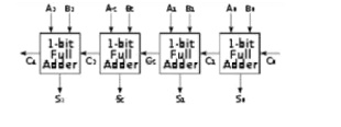
4-bit adder with logic gates shown
It is possible to create a logical circuit using multiple full adders to add N-bit numbers. Each full adder inputs a Cin, which is the Cout of the previous adder. This kind of adder is a ripple carry adder, since each carry bit "ripples" to the next full adder. Note that the first (and only the first) full adder may be replaced by a half adder.
The layout of ripple carry adder is simple, which allows for fast design time; however, the ripple carry adder is relatively slow, since each full adder must wait for the carry bit to be calculated from the previous full adder. The gate delay can easily be calculated by inspection of the full adder circuit. Each full adder requires three levels of logic. In a 32-bit [ripple carry] adder, there are 32 full adders, so the critical path (worst case) delay is 31 * 2(for carry propagation) + 3(for sum) = 65 gate delays.
Carry look-ahead adders
Main article: Carry look-ahead adder
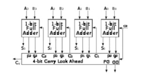
4-bit adder with Carry Look Ahead
To reduce the computation time, engineers devised faster ways to add two binary numbers by using carry lookahead adders. They work by creating two signals (P and G) for each bit position, based on whether a carry is propagated through from a less significant bit position (at least one input is a '1'), a carry is generated in that bit position (both inputs are '1'), or if a carry is killed in that bit position (both inputs are '0'). In most cases, P is simply the sum output of a half-adder and G is the carry output of the same adder. After P and G are generated the carries for every bit position are created. Some advanced carry look ahead architectures are the Manchester carry chain, Brent-Kung adder, and the Kogge-Stone adder.
Some other multi-bit adder architectures break the adder into blocks. It is possible to vary the length of these blocks based on the propagation delay of the circuits to optimize computation time. These block based adders include the carry bypass adder which will determine P and G values for each block rather than each bit, and the carry select adder which pre-generates sum and carry values for either possible carry input to the block.
Other adder designs include the conditional sum adder, carry skip adder, and carry complete adder.
Lookahead Carry Unit
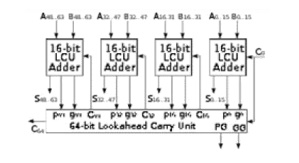
A 64-bit adder
By combining multiple carry look-ahead adders even larger adders can be created. This can be used at multiple levels to make even larger adders. For example, the following adder is a 64-bit adder that uses four 16-bit CLAs with two levels of LCUs.
compressors
We can view a full adder as a 3:2 compressor: it sums three one-bit inputs, and returns the result as a single two-bit number. Thus, for example, an input of 101 results in an output of 1+0+1=10 (2). The carry-out represents bit one of the result, while the sum represents bit zero. Likewise, a half adder can be used as a 2:2 compressor.
compressors can be used to speed up the summation of three or more addends. If the addends are exactly three, the layout is known as the carry-save adder. If the addends are four or more, more than one layer of compressors is necessary and there are various possible design for the circuit: the most common are Dadda and Wallace trees. This kind of circuit is most notably used in multipliers, which is why these circuits are also known as Dadda and Wallace multipliers.
Multiplexer
In electronics, a multiplexer or mux (occasionally the terms muldex or muldem are also found[1] for a combination multiplexer-demultiplexer) is a device that performs multiplexing; it selects one of many analog or digital input signals and forwards the selected input into a single line. A multiplexer of 2n inputs has n select lines, which are used to select which input line to send to the output.
An electronic multiplexer makes it possible for several signals to share one device or resource, for example one A/D converter or one communication line, instead of having one device per input signal.
On the other end, a demultiplexer (or demux) is a device taking a single input signal and selecting one of many data-output-lines, which is connected to the single input. A multiplexer is often used with a complementary demultiplexer on the receiving end.
An electronic multiplexer can be considered as a multiple-input, single-output switch, and a demultiplexer as a single-input, multiple-output switch. The schematic symbol for a multiplexer is an isosceles trapezoid with the longer parallel side containing the input pins and the short parallel side containing the output pin. The schematic on the right shows a 2-to-1 multiplexer on the left and an equivalent switch on the right. The sel wire connects the desired input to the output.
In telecommunications, a multiplexer is a device that combines several input information signals into one output signal, which carries several communication channels, by means of some multiplex technique. A demultiplexer is in this context a device taking a single input signal that carries many channels and separates those over multiple output signals.
In telecommunications and signal processing, an analog time division multiplexer (TDM) may take several samples of separate analogue signals and combine them into one pulse amplitude modulated (PAM) wide-band analogue signal. Alternatively, a digital TDM multiplexer may combine a limited number of constant bit rate digital data streams into one data stream of a higher data rate, by forming data frames consisting of one timeslot per channel.
In telecommunications, computer networks and digital video, a statistical multiplexer may combine several variable bit rate data streams into one constant bandwidth signal, for example by means of packet mode communication. An inverse multiplexer may utilize several communication channels for transferring one signal.
Cost savings
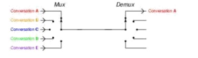
The basic function of a multiplexer: combining multiple inputs into a single data stream. On the receiving side, a demultiplexer splits the single data stream into the original multiple signals.
One use for multiplexers is cost savings by connecting a multiplexer and a demultiplexer (or demux) together over a single channel (by connecting the multiplexer's single output to the demultiplexer's single input). The image to the right demonstrates this. In this case, the cost of implementing separate channels for each data source is more expensive than the cost and inconvenience of providing the multiplexing/demultiplexing functions. In a physical analogy, consider the merging behaviour of commuters crossing a narrow bridge; vehicles will take turns using the few available lanes. Upon reaching the end of the bridge they will separate into separate routes to their destinations.
At the receiving end of the data link a complementary demultiplexer is normally required to break single data stream back down into the original streams. In some cases, the far end system may have more functionality than a simple demultiplexer and so, while the demultiplexing still exists logically, it may never actually happen physically. This would be typical where a multiplexer serves a number of IP network users and then feeds directly into a router which immediately reads the content of the entire link into its routing processor and then does the demultiplexing in memory from where it will be converted directly into IP packets.
Often, a multiplexer and demultiplexer are combined together into a single piece of equipment, which is usually referred to simply as a "multiplexer". Both pieces of equipment are needed at both ends of a transmission link because most communications systems transmit in both directions.
A real world example is the creation of telemetry for transmission from the computer/instrumentation system of a satellite, space craft or other remote vehicle to a ground-based system.
In analog circuit design, a multiplexer is a special type of analog switch that connects one signal selected from several inputs to a single output.
Digital multiplexers
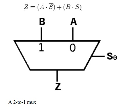
In digital circuit design, the selector wires are of digital value. In the case of a 2-to-1 multiplexer, a logic value of 0 would connect I0 to the output while a logic value of 1 would connect I1 to the output. In larger multiplexers, the number of selector pins is equal to [log2(n)] where is the number of inputs.
For example, 9 to 16 inputs would require no fewer than 4 selector pins and 17 to 32 inputs would require no fewer than 5 selector pins. The binary value expressed on these selector pins determines the selected input pin.
A 2-to-1 multiplexer has a boolean equation where A and F are the two inputs, s is the selector input, and Z is the output:
Which can be expressed as a truth table:
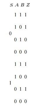
This truth table shows that when S=0 then Z=A but when S=1 then S=B. A straightforward realization of this 2-to-1 multiplexer would need 2 AND gates, an OR gate, and a NOT gate.
Larger multiplexers are also common and, as stated above, requires [log2(n)] selector pins for n inputs. Other common sizes are 4-to-1, 8-to-1, and 16-to-1. Since digital logic uses binary values, powers of 2 are used (4, 8, 16) to maximally control a number of inputs for the given number of selector inputs.
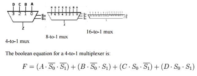
Two realizations for creating a 4-to-1 multiplexer are shown below:
These are two realizations of a 4-to-1 multiplexer:
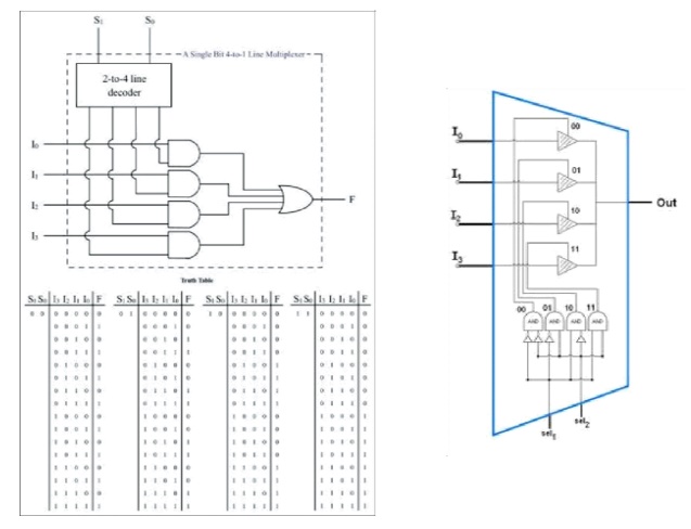
one realized from a decoder, AND gates, and an OR gate
· one realized from 3-state buffers and AND gates (the AND gates are acting as the decoder)
Note that the subscripts on the In inputs indicate the decimal value of the binary control inputs at which that input is let through.
Chaining multiplexers
Larger multiplexers can be constructed by using smaller multiplexers by chaining them together. For example, an 8-to-1 multiplexer can be made with two 4-to-1 and one 2-to-1 multiplexers. The two 4-to-1 multiplexer outputs are fed into the 2-to-1 with the selector pins on the 4-to-1's put in parallel giving a total number of selector inputs to 3, which is equivalent to an 8-to-1.
Digital demultiplexers
Demultiplexers take one data input and a number of selection inputs, and they have several outputs. They forward the data input to one of the outputs depending on the values of the selection inputs. Demultiplexers are sometimes convenient for designing general purpose logic, because if the demultiplexer's input is always true, the demultiplexer acts as a decoder. This means that any function of the selection bits can be constructed by logically OR-ing the correct set of outputs.
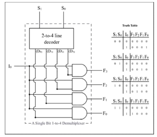
Example: A Single Bit 1-to-4 Line Demultiplexer
Multiplexers as PLDs
Multiplexers can also be used as programmable logic devices. By specifying the logic arrangement in the input signals, a custom logic circuit can be created. The selector inputs then act as the logic inputs. This is especially useful in situations when cost is a factor and for modularity.
Decoder
A decoder is a device which does the reverse of an encoder, undoing the encoding so that the original information can be retrieved. The same method used to encode is usually just reversed in order to decode.
In digital electronics, a decoder can take the form of a multiple-input, multiple-output logic circuit that converts coded inputs into coded outputs, where the input and output codes are different. e.g. n-to-2n, binary-coded decimal decoders. Enable inputs must be on for the decoder to function, otherwise its outputs assume a single "disabled" output code word. Decoding is necessary in applications such as data multiplexing, 7 segment display and memory address decoding.
The example decoder circuit would be an AND gate because the output of an AND gate is "High" (1) only when all its inputs are "High." Such output is called as "active High output". If instead of AND gate, the NAND gate is connected the output will be "Low" (0) only when all its inputs are "High". Such output is called as "active low output".
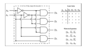
Example: A 2-to-4 Line Single Bit Decoder
A slightly more complex decoder would be the n-to-2n type binary decoders. These type of decoders are combinational circuits that convert binary information from 'n' coded inputs to a maximum of 2n unique outputs. We say a maximum of 2n outputs because in case the 'n' bit coded information has unused bit combinations, the decoder may have less than 2n outputs. We can have 2-to-4 decoder, 3-to-8 decoder or 4-to-16 decoder. We can form a 3-to-8 decoder from two 2-to-4 decoders (with enable signals).
Similarly, we can also form a 4-to-16 decoder by combining two 3-to-8 decoders. In this type of circuit design, the enable inputs of both 3-to-8 decoders originate from a 4th input, which acts as a selector between the two 3-to-8 decoders. This allows the 4th input to enable either the top or bottom decoder, which produces outputs of D(0) through D(7) for the first decoder, and D(8) through D(15) for the second decoder.
A decoder that contains enable inputs is also known as a decoder-demultiplexer. Thus, we have a 4-to-16 decoder produced by adding a 4th input shared among both decoders, producing 16 outputs.
Row select
Most kinds of random-access memory use a n-to-2n decoder to convert the selected address on the address bus to one of the row address select lines. A decoder is a device which does the reverse of an encoder, undoing the encoding so that the original information can be retrieved. The same method used to encode is usually just reversed in order to decode.
In digital electronics, a decoder can take the form of a multiple-input, multiple-output logic circuit that converts coded inputs into coded outputs, where the input and output codes are different. e.g. n-to-2n, binary-coded decimal decoders. Enable inputs must be on for the decoder to function, otherwise its outputs assume a single "disabled" output code word. Decoding is necessary in applications such as data multiplexing, 7 segment display and memory address decoding.
The example decoder circuit would be an AND gate because the output of an AND gate is "High" (1) only when all its inputs are "High." Such output is called as "active High output". If instead of AND gate, the NAND gate is connected the output will be "Low" (0) only when all its inputs are "High". Such output is called as "active low output". Example: A 2-to-4 Line Single Bit Decoder
A slightly more complex decoder would be the n-to-2n type binary decoders. These type of decoders are combinational circuits that convert binary information from 'n' coded inputs to a maximum of 2n unique outputs. We say a maximum of 2n outputs because in case the 'n' bit coded information has unused bit combinations, the decoder may have less than 2n outputs. We can have 2-to-4 decoder, 3-to-8 decoder or 4-to-16 decoder. We can form a 3-to-8 decoder from two 2-to-4 decoders (with enable signals).
Similarly, we can also form a 4-to-16 decoder by combining two 3-to-8 decoders. In this type of circuit design, the enable inputs of both 3-to-8 decoders originate from a 4th input, which acts as a selector between the two 3-to-8 decoders. This allows the 4th input to enable either the top or bottom decoder, which produces outputs of D(0) through D(7) for the first decoder, and D(8) through D(15) for the second decoder.
A decoder that contains enable inputs is also known as a decoder-demultiplexer. Thus, we have a 4-to-16 decoder produced by adding a 4th input shared among both decoders, producing 16 outputs. [edit] Row select
Instruction decoder
In CPU design, the instruction decoder is the part of the CPU that converts the bits stored in the instruction register -- or, in CPUs that have microcode, the microinstruction -- into the control signals that control the other parts of the CPU.
A simple CPU with 8 registers may use 3-to-8 logic decoders inside the instruction decoder to select two source registers of the register file to feed into the ALU as well as the destination register to accept the output of the ALU. A typical CPU instruction decoder also includes several other things.
Related Topics