Chapter: VLSI Design : Combinational and Sequential Circuit Design
Circuit Families and Its Comparison
CIRCUIT FAMILIES AND ITS
COMPARISON
The
method of logical effort does not apply to arbitrary transistor networks, but
only to logic gates. A logic gate has one or more inputs and one output,
subject to the following restrictions:
The gate
of each transistor is connected to an input, a power supply, or the output; and
Inputs are connected only to transistor gates.
The first
condition rules out multiple logic gates masquerading as one, and the second
keeps inputs from being connected to transistor sources or drains, as in
transmission gates without explicit drivers.
1. PSEUDO-NMOS Circuits
Static
CMOS gates are slowed because an input must drive both NMOS and PMOS
transistors.
In any
transition, either the pullup or pulldown network is activated; meaning the
input capacitance of the inactive network loads the input.
Moreover,
PMOS transistors have poor mobility and must be sized larger to achieve
comparable rising and falling delays, further increasing input capacitance.
Pseudo-NMOS
and dynamic gates offer improved speed by removing the PMOS transistors from
loading the input.
This
section analyzes pseudo-NMOS gates, while section 10.2 explores dynamic logic.
Pseudo-NMOS gates resemble static gates, but replace the slow PMOS pullup stack
with a single grounded PMOS transistor which acts as a pullup resistor.
The
effective pullup resistance should be large enough that the NMOS transistors
can pull the output to near ground, yet low enough to rapidly pull the output
high.
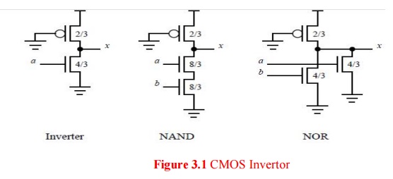
Figure
shows several pseudo-NMOS gates ratioed such that the pulldown transistors are
about four times as strong as the pullup.
The logical
effort follows from considering the output current and input capacitance
compared to the reference inverter from Figure Sized as shown, the PMOS
transistors produce 1/3 of the current of the reference inverter and the NMOS
transistor stacks produce 4/3 of the current of the reference inverter.
For
falling transitions, the output current is the pulldown current minus the
pullup current which is fighting the pulldown,For rising transitions, the
output current is just the pullup current, 1/3.
The
inverter and NOR gate have an input capacitance of 4/3. The falling logical
effort is the input capacitance divided by that of an inverter with the same
output current, or The rising logical effort is three times greater, because
the current produced on a rising transition is only one third that of a falling
transition. The average logical effort is g = (4=9+4=3)=2 = 8.
This
neither is independent of the number of inputs, explaining why pseudo-NMOS is a
way to build fast wide NOR gates. Table shows the rising, falling, and average
logical efforts of other pseudo-NMOS gates, assuming _ = 2 and a 4:1 pulldown
to pullup strength ratio.
Comparing
this with Table shows that pseudo-NMOS multiplexers are slightly better than
CMOS multiplexers and that pseudo-NMOS NAND gates are worse than CMOS NAND
gates.
Since
pseudo- NMOS logic consumes power even when not switching, it is best used for
critical NOR functions where it shows greatest advantage.
Similar
analysis can be used to compute the logical effort of other logic technologies,
such as classic NMOS and bipolar and GaAs.
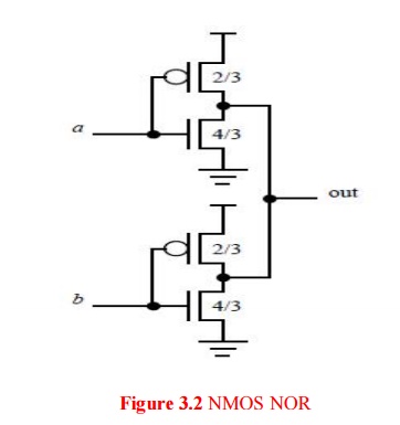
2. Symmetric NOR gates
Johnson
proposed a novel structure for a 2-input NOR, shown in Figure. The gate
consists of two inverters with shorted outputs, ratioed such that an inverter
pulling down can overpower an inverter pulling up.
This
ratio is exactly the same as is used for pseudo-NMOS gates. The difference is
that when the output should rise, both inverters pull up in parallel, providing
more current than is available from a regular pseudo-NMOS pullup.
The
worst-case pulldowncurrent is equal to that of a unit inverter, as we had found
in the analysis of pseudo-NMOS NOR gates. The pullup current comes from two
PMOS transistors in parallel and is thus 2=3 that of a unit inverter.
Therefore, the logical effort is 2=3 for a falling output and 1 for a rising
output.
The
average effort is g = 5=6, which is better than that of a pseudo-NMOS NOR and
far superior to that of a static CMOS NOR and even for NAND gates.
3. Domino circuits
Pseudo-NMOS
gates eliminate the bulky PMOS transistors loading the inputs, but pay the
price of quiescent power dissipation and contention between the pullup and
pulldown transistors.
Dynamic
gates offer even better logical effort and lower power consumption by using a
clocked precharge transistor instead of a pullup that is always conducting. The
dynamic gate is precharged HIGH then may evaluate LOW through an NMOS stack.
Unfortunately,
if one dynamic inverter directly drives another, a race can corrupt the result.
When the clock rises, both outputs have been precharged HIGH.
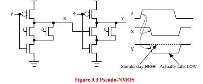
The HIGH
input to the first gate causes its output to fall, but the second gate’s output
also falls in response to its initial HIGH input. The circuit therefore
produces an incorrect result because the second output will never rise during
evaluation, as shown in Figure.
Domino
circuits solve this problem by using inverting static gates between dynamic
gates so that the input to each dynamic gate is initially LOW.
The
falling dynamic output and rising static output ripple through a chain of gates
like a chain of toppling dominos.
Domino
logic runs 1:5 to 2 times faster than static CMOS logic because dynamic gates
present a much lower input capacitance for the same output current and have a
lower switching threshold, and because the inverting static gate can be skewed
to favor the critical monotonically rising evaluation edges.
Figure
shows some domino gates. Each domino gate consists of a dynamic gate followed
by an inverting static gate1.
The
static gate is often but not always an inverter. Since the dynamic gate’s
output falls monotonically during evaluation, the static gate should be skewed
high to favor its monotonically rising output.
We have
calculated the logical effort of high-skew gates in Table and will compute the
logical effort of dynamic gates in the next section.
The
logical effort of a domino gate is then the product of the logical effort of
the dynamic gate and of the high-skew gate. Remember that a domino gate counts
as two stages when choosing the best number of stages.
A dynamic
gate may be designed with h or without a clocked evaluation transistor; the
extra transistor slows the gate but eliminates any path between power and
ground during p recharge when the inputs are still high.
Some
dynamic gates include weak PMOS transistors called keepers so that the dynamic
output will remain driven if the clock stops high. Domino designers face a
number of questions when selecting a circuit topology.
How many
stages should be used? Should the static gates be inverters, or should they
perform logic? How should precharge transistors and keepers be sized? What is
the benefit of removing the clocked evaluation transistors? We will show that
domino logic should be designed with a stage effort of 2–2:75, rather than 4
that we found for static logic.
Therefore,
paths tend to use more stages and it is rarely beneficial to perform logic with
the inverting static gates.
Related Topics