Phase Locked Loop (PLL) - Voltage Controlled Oscillator | Linear Integrated Circuits : Analog Multiplier and PLL
Chapter: Linear Integrated Circuits : Analog Multiplier and PLL
Voltage Controlled Oscillator
Voltage
Controlled Oscillator:
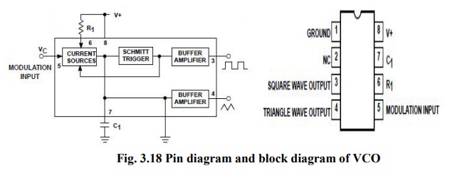
Referring
to the circuit in the above figure, the capacitor c1 is linearly charged or
discharged by a constant current source/sink. The amount of current can be
controlled by changing the voltage vc applied at the modulating input (pin 5)
or by changing the timing resistor R1 external to the IC chip. The
voltage at pin 6 is held at the same voltage as pin 5.
Thus, if the modulating voltage at pin 5 is increased, the voltage at pin 6 also increases, resulting in less voltage across R1 and thereby decreasing the charging current.
The
voltage across the capacitor C1 is applied to the inverting input
terminal of Schmitt trigger via buffer amplifier. The output voltage swing of
the Schmitt trigger is designed to Vcc and 1.5 Vcc. If Ra = Rb
in the positive feedback loop, the voltage at the non-inverting input terminal
of Schmitt trigger swings from 0.5 Vcc to 0.25 Vcc.
When
the voltage on the capacitor c1 exceeds 0.5 Vcc during charging, the output of
the Schmitt trigger goes LOW (0.5 Vcc). The capacitor now discharges and when
it is at 0.25 Vcc, the output of Schmitt trigger goes HIGH (Vcc). Since the
source and sink currents are equal, capacitor charges and discharges for the
same amount of time. This gives a triangular voltage waveform across c1 which
is also available at pin 4.
The
square wave output of the Schmitt trigger is inverted by buffer amplifier at
pin 3. The output waveforms are shown near the pins 4 and 3.
The
output frequency of the VCO can be given as follows:
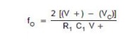
where
V+ is Vcc.
The
output frequency of the VCO can be changed either by (i) R1, (ii) c1
or (iii) the voltage vc at the modulating input terminal pin 5. The voltage vc
can be varied by connecting a R1R2 circuit as shown in
the figure below. The components R1and c1 are first selected so that VCO output
frequency lies in the centre of the operating frequency range.
Now
the modulating input voltage is usually varied from 0.75 Vcc to Vcc which can
produce a frequency variation of about 10 to 1.
The
signetics NE/SE 560 series is monolithic phase locked loops. The SE/NE 560,
561, 562, 564, 565 & 567 differ mainly in operating frequency range, poser
supply requirements & frequency & bandwidth adjustment ranges.
Related Topics