Chapter: Digital Logic Circuits : Number Systems and Digital Logic Families
TTL
TTL
The original basic transistor- transistor logic (TIL) gute was a slight improvement over the DTL gate. As TIL technology progressed. improvements were added to the point where this logic family became widely used in the design of digital systems. Today. ~1 0 S and C ~ IOS logic. which will be discussed in Sections 10.7 and 10.8. are the dominant technologies in VLSI circuits.
There are several subfamilies or series of the TTL technology. The names and characteristics of eight TIL series appear in Table 10.2. Commercial TIL ICs have a number designation that starts with 74 and follows with a suffix that identifies the series. Examples are 740·t 74S86. and 74ALS161. Fan-out. power dissipation. and propagation delay were defined in Section The speed-power product is an important parameter used in comparing the various TIL series. The product of the propagation delay and power dissipation. the speed-power product is measured in picojoules (pJ ).A low value for this parameter is desirable. because it indicates that a given propagation delay can beachieved without excessive power dissipation. and vice versa.
The standard TIL gate was the first version in theTIL family. This basic gate v. as then designed with different resistor values to produce gates with lower power dissipation or with higher speed. The propagation delay of a transistor circuit that goes into saturation depends mostly on two factors: storage time and RC time constants. Reducing the storage time decreases he propagation delay. Reducing resistor values in the circuit reduces the RCtime constants and decreases the propagation delay. Of course. the trade-off is higher power dissipation. because lower resistances draw more current from the power supply. The speed of the gate is inversely proportional to the propagation delay.
In the low-power TIL gate. the resistor values are higher than in the standard gate in order to reduce the power dissipation. but the propagation delay is increased. In the high-speed TTL gate. resistor values are lowered to reduce the propagation delay. but the power dissipation is increased. The Schottky TTL gate was the next improvement in the technology. The effect of the Schottky transistor is to remove the storage time delay by preventing the transistor from going into saturation. This series increases the speed of operation of the circuit without an excessive increase in power dissipation. The low-power Schottky TTL sacrifices some speed for reduced power dissipation . It is equal to the standard TTL in propagation delay, but has only one-fifth the power dissipat ion. Further innovations led to the development of the advanced Schottky series, which provides an improvement in propagation delay over the Schottky series and also lowers the power dissipation. The advanced low-power Schottky has the lowest speed-power product and is the most efficient series. The fast TTL family is the best choice for high-speed designs. All TTL series are available in S81 components and in more complex forms. such as MSI and LSI components. The differences in the TTL series are not in the digital logic that they perform, but rather in the internal construction of the basic NAND gale. In any case, TTL gates in all the available series come in three different types of output configuration:
1. Open-collector output
2. Totem-pole output
3. Three-state output
These three types of outputs are considered next, in conjunction with the circuit description of the basic TTL gate.
Open-Collector Output Gate
The basic TIL gate shown in Fig. 10.11 is a modified circuit of the D'Tt.gate. The multiple emitters in transistor QI are connected to the inputs, Most of the time, these emitters behave like the input diodes in the DTL gate, since they form a pn junction with their common base. The base-collector junction of QJ acts as another pI! junction diode corresponding to DJ in the
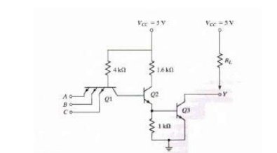
DTL gate Transistor Q2 repl aces the second diode. D2. in the DTL gale. The output of the TTL gate is taken from the open collector of Q3. A resistor connected to l ec must be inserted externally to the Ie package for the output to "pull up" to the high voltage level when Q3 is off; otherwise. the Output acts as an open circuit. The reason for not providing the resistor intern ally will be discussed later.
The two voltage levels of the TTL gate are 0.2 V for the low level and from ~ ,~ to 5 v for the high level. The basic circuit is a ~AND gate, If any input is low. the corresponding base-emitter junction in QJis forward biased. The voltage at the base of QJ is equal to the input voltage of 0.2 V pl u ~ a VHE drop of 0.7. or 0.9 V, In order for Q3 to start on ducting. the path from QJto Q3 must overcome a potential of one diode drop in the base-collector pn junction of QJ and two VBE drops in Q2 andQ3. or 3 x 0"6 = 1.8 V. Since the base of QI is maintained at 0.9 V by the input signal. the output transistor cannot conduct and is cut off. The output level will be high if an external resistor is connected between the output and vee(or an open circuit if a resistor is not used).
If all inputs are high. both Q2 and Q3 conduct and saturate. The base voltage of QJ is equal to the volt age across its base-collector pn j unction plus IWO VHE drops in Q2 and QJ. or about 0.7 x 3 = 2.1 V. Since all inputs are high and greater than 2.4 V. the base-emitter junctions of Q1 are all reverse biased. When output transistor QJ saturates (provided that it has a current path). the output voltage goes low to 0.2 V. This confirms the conditions of a NAND operation. In the analysis presented thus far. we said that the base-collector junction of QJ act s like a pn diode junction. This is true in the steady-state condition. However. duri ng the turnoff transition. Ql doe s exhibit transistor action. resulting in a reduction in propagation delay .When all inputs are high and then one of the inputs Is brought to a low level. both Q2 and Q3 start turning off.At this time. the collector j unction of QJ is reverse biased and the emitter is forward biased. so transistor QJ goes momentarily into the active region. The collector current of QJcomes from the base of Q2 and qu ick ly removes the noise immunity encountered. Without an external resistor. the output of the gate will be an open circuit when QJ is off. An open circuit 10an input of a TTL gate behaves as if it has a high level input (but a small amount of noise can change this to a low level) "when Q3 conducts, its collector will have a current path supplied by the input of the loading gate through Vee. The 4-k. 0 resistor. and the forward-biased base-emitter junction " Open-collector gales are used in three major applications: driving a lamp or relay. Performing wired logic. and constructing a common-bus system. An open-collector output can drive a lamp placed in its output through a limiting resistor. When the output is low. the saturated trasistor QJ forms a path for the current that turns the lamp on. When the output transistor is off. the lamp turn s off because there is no path for the current.
Related Topics