Chapter: Electronic Circuits : Wave Shaping and Multivibrator Circuits
Schmitt Trigger
Schmitt Trigger
Sometimes an input signal to a digital circuit
doesn't directly fit the description of a digital signal. For various reasons
it may have slow rise and/or fall times, or may have acquired some noise that
could be sensed by further circuitry. It may even be an analog signal whose
frequency we want to measure. All of these conditions, and many others, require
a specialized circuit that will "clean up" a signal and force it to
true digital shape.
The required circuit is called a Schmitt Trigger. It has two possible states just like other multivibrators. However, the trigger for this circuit to change states is the input voltage level, rather than a digital pulse. That is, the output state depends on the input level, and will change only as the input crosses a pre- defined threshold.
Unlike the other multivibrators you have built
and demonstrated, the Schmitt Trigger makes its feedback connection through the
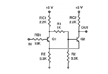
emitters of the transistors as shown in the schematic diagram to the right.
This makes for some useful possibilities, as we will see during our discussion of
the operating theory of this circuit.
To understand how this circuit works, assume
that the input starts at ground, or 0 volts. Transistor Q1 is necessarily
turned off, and has no effect on this circuit. Therefore, RC1, R1, and R2 form
a voltage divider across the 5 volt powersupply to set the base voltage of Q2
to a value of (5 × R2)/(RC1 + R1 + R2). Ifwe assume that the two transistors
are essentially identical, then as long as the input voltage remains
significantly less than the base voltage of Q2, Q1 will remain off and the
circuit operation will not change.
While Q1 is off, Q2 is on. Its emitter and
collector current are essentially the same, and are set by the value of RE and
the emitter voltage, which will be less than the Q2 base voltage by VBE.
If Q2 is in saturation under these circumstances, the output voltage will be
within a fraction of the threshold voltage set by RC1, R1, and R2. It is
important to note that the output voltage of this circuit cannot drop to zero
volts, and generally not to a valid logic 0. We can deal with that, but we must
recognize this fact.
Now, suppose that the input voltage rises, and
continues to rise until it approaches the threshold voltage on Q2's base. At
this point, Q1 begins to conduct. Since it now carries some collector current,
the current through RC1 increases and the voltage at the collector of Q1
decreases. But this also affects our voltage divider, reducing the base voltage
on Q2. But since Q1 is now conducting it carries some of the current flowing
through RE, and the voltage across RE doesn't change as rapidly. Therefore, Q2
turns off and the output voltage rises to +5 volts. The circuit has just
changed states.
If the input voltage rises further, it will
simply keep Q1 turned on and Q2 turned off. However, if the input voltage
starts to fall back towards zero, there must clearly be a point at which this
circuit will reset itself. The question is, What is the falling threshold
voltage? It will be the voltage at which Q1's base becomes more negative than Q2's
base, so that Q2 will begin conducting again. However, it isn't the same as the
rising threshold voltage, since Q1 is currently affecting the behavior of the
voltage divider.
We won't go through all of the derivation here,
but when VIN becomes equal to Q2's base voltage, Q2's base voltage
will be:
As VIN approaches this value, Q2
begins to conduct, taking emitter current away from Q1. This reduces the
current through RC1 which raises Q2's base voltage further, increasing Q2's
forward bias and decreasing Q1's forward bias. This in turn will turn off Q1,
and the circuit will switch back to its original state.
Three factors must be recognized in the Schmitt
Trigger. First, the circuit will change states as VIN approaches VB2,
not when the two voltages are equal. Therefore VB2 is very close to
the threshold voltage, but is not precisely equal to it. For example, for the
component values shown above, VB2 will be 2.54 volts when Q1 is held
off, and 2.06 volts as VIN is falling towards this value.
Second, since the common emitter connection is
part of the feedback system in this circuit, RE must be large enough to provide
the requisite amount of feedback, without becoming so large as to starve the
circuit of needed current. If RE is out of range, the circuit will not operate
properly, and may not operate as anything more than a high-gain amplifier over
a narrow input voltage range, instead of switching states.
The third factor is the fact that the output
voltage cannot switch over logic levels, because the transistor emitters are
not grounded. If a logic-level output is required, which is usually the case,
we can use a circuit such as the one shown here to correct this problem. This
circuit is basically two RTL inverters, except that one uses a PNP transistor. This
works because when Q2 above is turned off, it will hold a PNP inverter off, but
when it is on, its output will turn the PNP transistor on. The NPN transistor
here is a second inverter to re-invert the signal and to restore it to active
pull-down in common with all of our other logic circuits.
The circuit you will construct for this
experiment includes both of the circuits shown here, so that you can monitor
the response of the Schmitt trigger with L0.
Schmitt
Waveform Generators
Simple Waveform
Generators can be constructed using basic Schmitt trigger action Inverters
such as the TTL 74LS14. This method is by far the easiest way to make a basic
astable waveform generator. When used to produce clock or timing signals, the
astable multivibrator must produce a stable waveform that switches quickly
between its "HIGH" and "LOW" states without any distortion
or noise, and Schmitt inverters do just that.
We know that the output state of a Schmitt
inverter is the opposite or inverse to that of its input state, (NOT Gate
principles) and that it can change state at different voltage levels giving it
"hysteresis". Schmitt inverters use a Schmitt Trigger action that
changes state between an upper and a lower threshold level as the input voltage
signal increases and decreases about the input terminal. This upper threshold
level "sets" the output and the lower threshold
level"resets" the output which equates to a logic "0" and a
logic "1" respectively for an inverter. Consider the circuit below.
TTL
Schmitt Waveform Generator
The circuit consists simply of a TTL 74LS14
Schmitt inverter logic gate with a capacitor, C connected between its input
terminal and ground, (0v) with the positive feedback required for the circuit
to oscillate is provided by the feedback resistor, R. So how does it work?.
Assume that the charge across the capacitors plates is below the Schmitt's
lower threshold level of 0.8 volt (Datasheet value). This therefore makes the
input to the inverter at a logic "0" level resulting in a logic
"1" output level (inverter principals). One side of the resistor R is
now connected to the logic "1" level (+5V) output while the other
side of the resistor is connected to the capacitor, C which is at a logic
"0" level (0.8v or below).
The capacitor now starts to charge up in a
positive direction through the resistor at a rate determined by the RC time
constant of the combination. When the charge across the capacitor reaches the
1.6 volt upper threshold level of the Schmitt trigger (Datasheet value) the
output from the Schmitt inverter changes rapidly from a logic level
"1" to a logic level "0" state and the current flowing
through the resistor changes direction.
This change now causes the capacitor that was
originally charging up through the resistor, R to begin to discharge itself
back through the same resistor until the charge across the capacitors plates
reaches the lower threshold level of 0.8 volts and the inverters output
switches state again with the cycle repeating itself over and over again as
long as the supply voltage is present.
So the capacitor, C is constantly charging and
discharging itself during each cycle between the upper and lower threshold
levels of the Schmitt inverter producing a logic level "1" or a logic
level "0" at the inverters output. However, the output square wave
signal is not symmetrical producing a duty cycle of about 33% or 1/3 as the
mark-to-space ratio between "HIGH" and "LOW" is 1:2
respectively due to the input gate characteristics of the TTL inverter.
The value of the feedback resistor, R MUST also
be kept low to below 1kΩfor the circuit to oscillate correctly, 220R
to 470R is good, and by varying the value of the capacitor, C to vary the
frequency. Also at high frequency levels the output waveform changes shape from
a square shaped waveform to a trapezoidal shaped waveform as the input
characteristics of the TTL gate are affected by the rapid charging and
discharging of the capacitor.
With a resistor value between: 100R to 1kΩ, and
a capacitor value of between: 1nF to 1000uF. This would give a frequency range
of between 1Hzto 1MHz, (high frequencies produce waveform distortion).
Related Topics