Chapter: Power Electronics : Power Semi Conductor Devices
Power BJT
POWER BJT
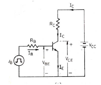
Power BJT means a large voltage blocking in the OFF state and high current carrying capability in the ON state. In most power application, base is the input terminal. Emitter is the common terminal. Collector is the output terminal.
1. Signal level of BJT
n+ doped emitter layer ,doping of base is more than collector.Depletion layer exists more towards the collector than emitter
2. Power BJT Construction
The maxium collector emitter voltage that can be sustained across the junction, when it is carrying substantial collector current.
Vceo=maxium collectorand emitter voltage that can be sustain by the device.
Vcbo=collector base breakdown voltage with emitter open
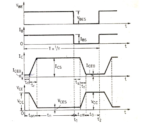
Primary Breakdown
It is due to convention avalanche breakdown of the C-B junction and its associated large flow of current.The thickness of the depletion region determines the breakdown voltage of the transistor.The base thickness is made as small as possible,in order to have good amplification capability. If the thickness is too small, the breakdown voltage is compromised.So a compromise has to be made between the two.
The Doping Levels
1.The doping of the emitter layer is quite large.
2.The base doping is moderate.
3.n- region is lightly doped.
4.n+ region doping level is similar to emitter.
1.Thickness Of Drift Region-It determines the breakdown length of the transistor. 2.The Base Thicknes -Small base thickness- good amplification capability
Too small base thickness- the breakdown voltage of the transistor has to be compromised. For a relatively thick base,the current gain will be relatively small.so it is increase the gain.Monolithicesigns for darlington connected BJT pair have been deveploed.
Secondary Breakdown
Secondary breakdown is due to large power disspation at localized site within the semi conductor.
Physics Of BJT Operation
The transistor is assumed to operate in active region. There is no doped collector drift region. It has importance only in switching operation, in active region of operation.
B-E junction is forward biased and C-B junction is reverse biased. Electrons are injected into base from the emitter. Holes are injected from base into the emitter.
Quasi Saturation
Intially we assume that, the transistor is in active region. Base current is allowed to increase then lets see what happens.first collector rises in response to base current. So there is a increase voltage drop across the collector load.So C-E voltage drops.
Because of increase in collector current, there is a increase in voltage in drift region. This eventually reduces the reverse biased across the C-B junction.so n-p junction get smaller, at some point the junction become forward bised. So now injection of holes from base into collector drift region occurs. Charge neutrality requires the electron to be injected in the drift region of the holes. From where these electron came. Since a large no of electron is supplied to the C-B junction via injection from emitter and subsequent diffusion across the base. As excess carrier build up in the drift region begins to occur quasi saturation region is entered. As the injected carrires increase in the drift region is gradually shotred out and the voltage across the drift region drops. In quasi saturation the drift region is not completely shorted out by high level injection. Hard saturation obtained when excess carrier density reaches the n+ side.
During quasi saturation, the rate of the collector fall.Hard saturation occurs when excess carriers have completely swept across the drift region.
Related Topics