Chapter: Electronic Devices and Circuits : Transistors
MOSFET (Metal Oxide Semiconductor Field Effect Transistor) - Depletion and Enhancement mode: Construction, Operation, Symbol, Characteristics
MOSFET (Metal Oxide Semiconductor Field Effect Transistor)
Like JFET, it has a source, Drain and Gate.
It is also called IGFET (Insulated Gate FET) because gate terminal is insulated from channel. Therefore it has extremely high input resistance.
Ø Types of MOSFET
It has two types
1. Depletion mode MOSFET
a. N-channel
b. P-channel
2. Enhancement mode MOSFET
a. N-channel
b. P-channel
The enhancement-type MOSFET is usually referred to as an E-MOSFET, and the depletion type, a D-MOSFET. The drain current in a MOSFET is controlled by the gate-source voltage VGS.
1. Depletion mode-MOSFET [D-MOSFET]
In depletion mode of operation the bias voltage on the gate reduce the number of charge carriers in the channel and therefore reduce the drain current ID.It operates in both depletion mode and enhancement mode.
Ø Symbol
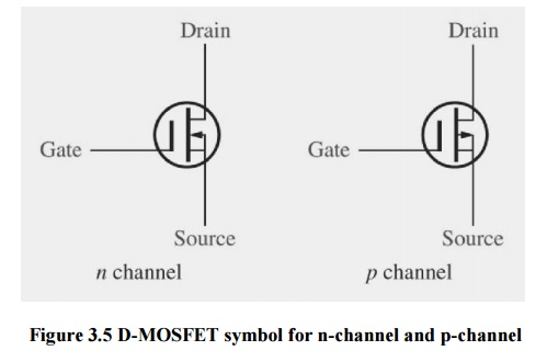
Construction
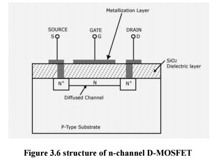
It consists of lightly doped p-type substrate in which two highly doped n-regions are diffused.
The source and drain terminals are connected through metallic contacts to n-doped regions linked by an n-channel. The gate is also connected to a metal contact surface but remains insulated from the n-channel by a very thin silicon dioxide (SiO2) layer. SiO2 is a particular type of insulator referred to as a dielectric that sets up opposing (as revealed by the prefix di-) electric fields within the dielectric when exposed to an externally applied field.
Then the thin layer of metal aluminium is formed over the Sio2 layer. This metal overs the entire channel region and it forms the gate(G).
Operation of N-channel D-MOSFET
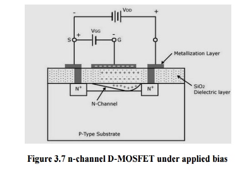
Case (i) “when and is increased from zero”
Here N-base (Drain) is connected to positive supply. It act as a reverse bias. Due to this, depletion region gets increases.
Free electron from n-channel are attracted towards positive potential of drain terminal. This establishes current through channel flows from drain to source and denoted as IDSS.
Pinch of voltage
The pinch off voltage is the voltage at which the junction is depleted of charge carriers.
Case (ii) “whenand is increased from zero”
The negative charge on gate repels conduction electrons from the channel and attract holes from the p-type substrate.
Due to this electron-hole recombination occurs and reduce the number of free electrons in the channel available for conduction, reducing Drain current (ID).
When negative voltage of is incresed the pinch of voltage decreased. When is further increased the channel is fully depleted and no current flows through it.
The negative voltage depletion MOSFET.
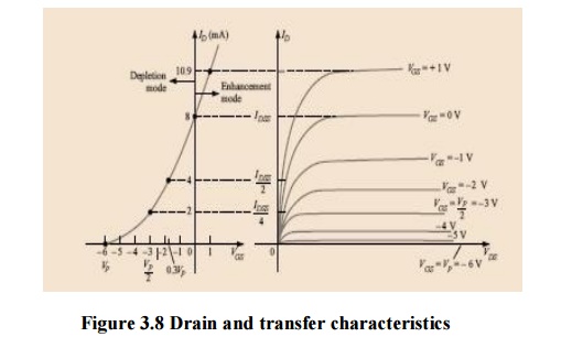
Ø Characteristics curve
Two types
Drain characteristics
Transfer characteristics
D-MOSFET‘s are biased to operate in two modes :depletion or enhancement mode.
2. ENHANCEMENT- MODE MOSFET [E-MOSFET]
o In this mode bias on the gate increases the number of charge carriers in the channel and increases the drain current (ID).
o It operates only in the enhancement mode and has no depletion mode of operation.It has no physical channel.
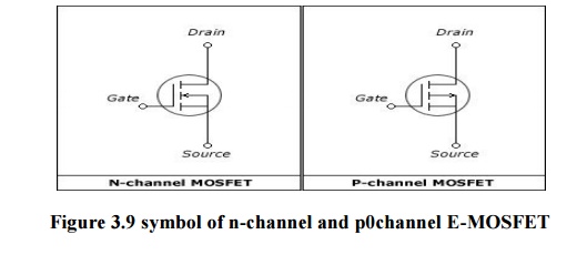
Ø Symbol of E-MOSFET
Ø Basic Construction
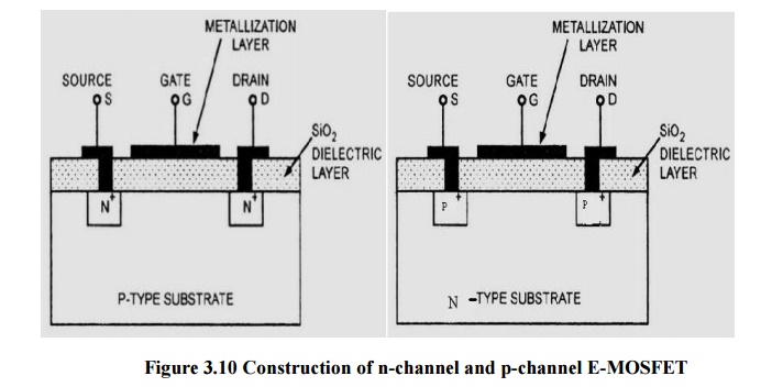
In the basic construction of the n-channel enhancement-type MOSFET, a slab of p-type material is formed from a silicon base and is again referred to as thesubstrate. As with the depletion-type MOSFET, the substrate is sometimes internally connected to the source terminal, while in other cases a fourth lead is made available for external control of its potential level.
The SiO2 layer is still present to isolate the gate metallic platform from the region between the drain and source, but now it is simply separated from a section of the p-type material.
In summary, therefore, the construction of an enhancement-type MOSFET is quite similar to that of the depletion-type MOSFET, except for the absence of a channel between the drain and source terminals.
Ø Operation
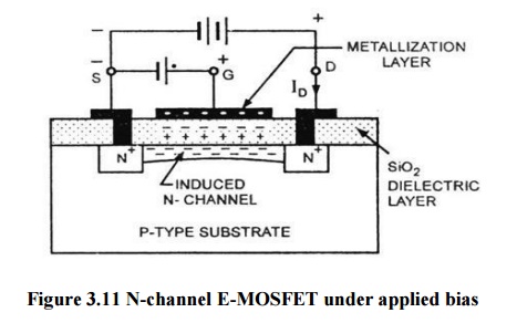
If VGS is set at 0 V and a voltage applied between the drain and source of the device, the absence of an n-channel (with its generous number of free carriers) will result in a current of effectively zero amperes—quite different from the depletion- type MOSFET and JFET where ID - IDSS.
It is not sufficient to saturation level as occurred for the JFET and depletion-type MOSFET.
The conductivity of the channel is enhanced by the positive bias voltage on the gate, the device is known as enhancement MOSFET. E-MOSFET‘s are normally called as ―OFF – MOSFET
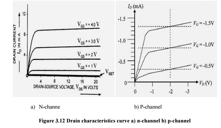
Ø Characteristics of E-MOSFET
Drain characteristics curve
Related Topics