Chapter: Digital Logic Circuits : Number Systems and Digital Logic Families
DTL Basic Gates
DTL Basic Gates
The basic circuit in the OTL digital
logic family is the NAND gate shown.Each input is associated with one diode.
The diodes and the 5·kO resistor from exor gate. The transistor serves as a
current amplifier while inverting the digital signal. The two voltage levels
are 0.2 V for the low level and between 4 and 5 V for the high level. The
analysis of the DTL gate should conform to the conditions listed in for the
NAND gate. If any input of the gale is low at 0.2 V. the corresponding input
diode conducts current through Vee
and the 5-kfl resistor into the input node . The voltage at point P is equal 10 the input voltage of 0.2 V
plus a diode drop of 0.7 V, for a total of 0.9 V. In order for the transiste r
to start conducting, the voltage at point P
must overcome (i.e., be at least as high as) a I·VBEdrop in QJ plus two
diode drops across DI and D2, or 3 X 0.6 = 1.8 V. Since the
voltage at P is maintained at 0.9 V
by the input conducting diode. the transistor is cut off with no drop across
the 2-kO resistor. and the output voltage is high at 5 V. If all input s of the
gate are high , the transistor is driven into the saturation region . The
voltage at P now is equal to VBE plus the two dio de drops across DI and D2, or0.7 X 3 = 2.1 V. Since all inputs are high at 5 V and since Vp = 2.1 V, the input diodes are reverse
biased and off. The base current is equal to the difference of the current s
flowing in the IWO 5·k n resistors and is sufficient to drive the transistor
into saturation. With the transistor saturated, the output drops to Va = 0.2 V, which is the low level for
the gate . The power dissipation of a DIL gate is about 12 mW and the
propagation delay averages 30 ns. The noise margin is about I V and a fan-out
as high as 8 is possible . The fan-out of the DIL gale is limited by the
maximum current that can flow in the collector of the saturated transistor. The
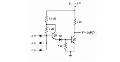
fan-out of a DTL gate may be increased by replacing one of the diodes in the
base circuit with a transistor, as shown in Fig. 10.10. Transistor Ql is maintained in the active region
when output transistor Q2 is
saturated. As a consequence, the modified circuit can supply a larger amount of
base current to the output transistor, which can now draw a larger amount of
collector current before it goes out of saturation . Part of the collector
current comes from the conducting diode s in the loading gates when Q2 is saturated. Thus, an increase in
the allow able saturated current in the collector allows more loads to be
connected to the output, increasing the fan-out capability of the gate
Related Topics