Chapter: High Voltage Engineering : Measurement of High Voltage and High Currents
Resistance Potential Dividers - Digital Techniques in High Voltage Measurement
DIGITAL TECHNIQUES IN HIGH
VOLTAGE MEASUREMENT
Resistance Potential Dividers
The
resistance potential dividers are the first to appear because of their
simplicity of construction, less space requirements, less weight and easy
portability. These can be placed near the test object which might not always be
confined to one location.
The
length of the divider depends upon two or three factors. The maximum voltage to
be measured is the first and if height is a limitation, the length can be based
on a surface flash over gradient in the order of 3–4 kV/cm irrespective of
whether the resistance R1 is of liquid or wire wound construction. The length
also depends upon the resistance value but this is implicitly bound up with the
stray capacitance of the resistance column, the product of the two (RC) giving
a time constant the value of which must not exceed the duration of the wave
front it is required to record. It is to be noted with caution that the
resistance of the potential divider should be matched to the equivalent
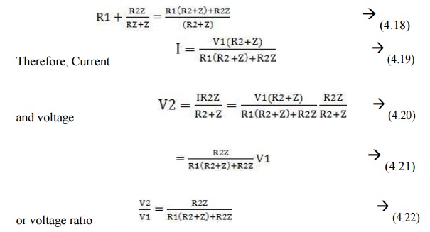
resistance of a given generator to obtain a given wave shape. FIG. 4.11 (a)
shows a common form of resistance potential divider used for testing purposes
where the wave front time of the wave is less than 1 micro sec.
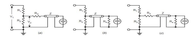
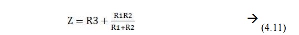
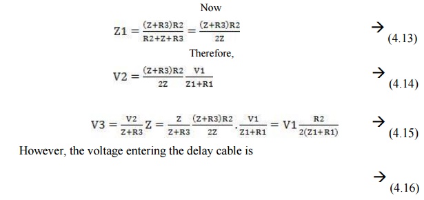
Figure: 4.11 various forms of resistance potential dividers recording circuits (a) Matching at divider
end (b) Matching at Oscillo graph end (c) Matching at both ends of delay cable
Here R3, the resistance at the divider end of the delay cable is
chosen such that R2 + R3 = Z which puts an upper limit on
R2 i.e., R2 < Z. In fact, sometimes the condition for matching is
given as
But,
since usually R1 > > R2, the above relation reduces
to Z = R3 + R2. From Fig. 4.19 (a), the voltage appearing
across R2 is

where Z1
is the equivalent impedance of R2 in parallel with (Z + R3),
the surge impedance of the cable being represented by an impedance Z to ground.
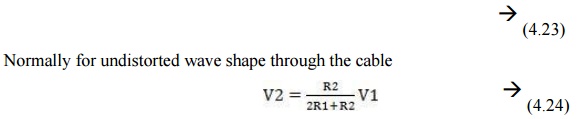
As this
voltage wave reaches the CRO end of the delay cable, it suffers reflections as
theimpedance offered by the CRO is infinite and as a result the voltage wave
transmitted into the CRO is doubled. The CRO, therefore, records a voltage The
reflected wave, however, as it reaches the low voltage arm of the potential
divider does not suffer any reflection as Z = R2 + R3 and
is totally absorbed by (R2 + R3). Since R2 is
smaller than Z and Z1 is a parallel combination of R2 and
(R3 + Z), Z1 is going to be smaller than R2
and since R1 > > R2, R1 will be much
greater than Z1 and, therefore to a first approximation Z1
+ R1 ≈ R1.
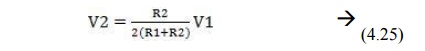
Fig. 4.11
(b) and (c) are the variants of the potential divider circuit of Fig. 4.11 (a).
The cable Matching is done by a pure ohmic resistance R4 = Z at the
end of the delay cable and, therefore, the voltage reflection coefficient is
zero i.e. the voltage at the end of the cable is transmitted completely into R4
and hence appears across the CRO plates without being reflected. As the input
impedance of the delay cable is R4 = Z, this resistance is a
parallel to
R2 and
forms an integral part of the divider’s low voltage arm. The voltage of such a
divider is, therefore, calculated as follows: Equivalent impedance
Due to
the matching at the CRO end of the delay cable, the voltage does not suffer any
reflection at that end and the voltage recorded by the CRO is given as
For a
given applied voltage V1 this arrangement will produce a smaller
deflection on the CRO Plates as compared to the one in Fig. 4.19 (a).The
arrangement of Fig. 4.19 (c) provides for matching at both ends of the delay
cable and is to be recommended where it is felt necessary to reduce to the
minimum irregularities produced in the delay cable circuit. Since matching is
provided at the CRO end of the delay cable, therefore, there is no reflection
of the voltage at that end and the voltage recorded will be half of that
recorded in the arrangement of Fig. 4.19 (a) viz
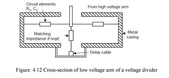
It is
desirable to enclose the low voltage resistance (s) of the potential dividers
in a metal screening box. Steel sheet is a suitable material for this box which
could be provided with a detachable closefitting lid for easy access. If there
are two low voltage resistors at the divider position as in Fig. 4.11 (a) and
(c), they should be contained in the screening box, as close together as
possible, with a removable metallic partition between them. The partition
serves two
purposes
(i) it acts as an electrostatic shield between the two resistors (ii) it
facilitates the changing of the resistors. The lengths of the leads should be
short so that practically no inductance
is contributed by these
leads. The screening
box should be
fitted with a
large earthling terminal. Fig. 4.12 shows a sketched cross-section of
possible layout for the low voltage arm of voltage divider.
Related Topics