Chapter: Measurements and Instrumentation : Transducers and Data Acquisition Systems
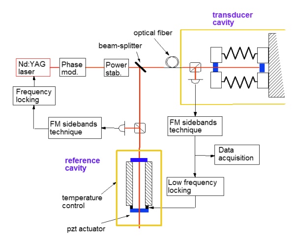
Optical Transducer

Optical Transducer
Transducer cavity:
A Fabry-Perot cavity between the bar and the resonant plate
Reference cavity:
A stable Fabry-Perot cavity acting as length reference
Laser source frequency locked to the reference cavity
General Architecture of smart sensor:
One can easily propose a general architecture of smart sensor from its definition, functions. From the definition of smart sensor it seems that it is similar to a data acquisition system, the only difference being the presence of complete system on a single silicon chip. In addition to this it has on–chip offset and temperature compensation. A general architecture of smart sensor consists of following important components:
· Sensing element/transduction element,
· Amplifier,
· Sample and hold,
· Analog multiplexer,
· Analog to digital converter (ADC),
· Offset and temperature compensation,
· Digital to analog converter (DAC),
· Memory,
· Serial communication and
· Processor
The generalized architecture of smart sensor is shown below:
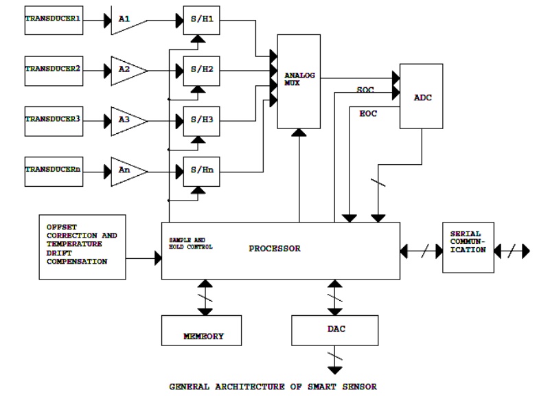
Architecture of smart sensor is shown. In the architecture shown A1, A2…An and S/H1, S/H2…S/Hn are the amplifiers and sample and hold circuit corresponding to different sensing element respectively. So as to get a digital form of an analog signal the analog signal is periodically sampled (its instantaneous value is acquired by circuit), and that constant value is held and is converted into a digital words. Any type of ADC must contain or proceeded by, a circuit that holds the voltage at the input to the ADC converter constant during the entire conversion time. Conversion times vary widely, from nanoseconds (for flash ADCs) to microseconds (successive approximation ADC) to hundreds of microseconds (for dual slope integrator ADCs). ADC starts conversion when it receives start of conversion signal (SOC) from the processor and after conversion is over it gives end of conversion signal to the processor. Outputs of all the sample and hold circuits are multiplexed together so that we can use a single ADC, which will reduce the cost of the chip. Offset compensation and correction comprises of an ADC for measuring a reference voltage and other for the zero. Dedicating two channels of the multiplexer and using only one ADC for whole system can avoid the addition of ADC for this. This is helpful in offset correction and zero compensation of gain due to temperature drifts of acquisition chain. In addition to this smart sensor also include internal memory so that we can store the data and program required.
Related Topics