Chapter: Advanced Computer Architecture : Multi-Core Architectures
IBM Cell Processor
IBM CELL
PROCESSOR
A chip
with one PPC hyper-threaded core called PPE and eight specialized cores called
SPEs.The challenge to be solved by the Cell was to put all those cores together
on a single chip. This was made possible by the use of a bus with outstanding
performance
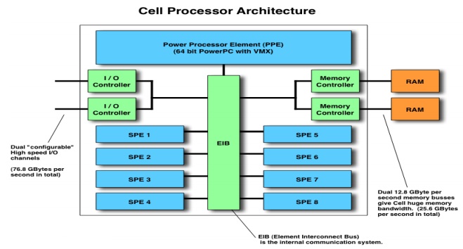
The Cell
processor can be split into four components:
Ø external
input and output structures,
Ø the main
processor called the Power Processing Element (PPE)
Ø eight
fully-functional co-processors called the Synergistic Processing Elements, or
SPEs,
Ø a
specialized high-bandwidth circular data bus connecting the PPE, input/output
elements and the SPEs, called the Element Interconnect Bus or EIB.
Overview of the architecture
of a Cell chip
POWERPC PROCESSOR ELEMENT:(PPE)
Ø The
PowerPC Processor Element, usually denoted as PPE is a dual-threaded powerpc
processor version 2.02.
Ø This
64-bit RISC processor also has the Vector/SIMD Multimedia Extension.
Ø The PPE’s
role is crucial in the Cell architecture since it is on the one hand running
the
OS, and
on the other hand controlling all other resources, including the SPEs .
Ø The PPE
is made out of two main units:
1: The
Power Processor Unit
2:The
Power Processor Storage Subsystem (PPSS).
PPE Block diagram
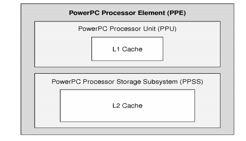
PPU:
It is the
processing part of the PPE and is composed of:
Ø A full
set of 64-bit PowerPC registers.
Ø 32
128-bit vector multimedia registers.
Ø A 32KB L1
instruction cache.
Ø A 32KB L1
data cache.
All the
common components of a ppc processors with vector/SIMD extensions (instruction
control unit, load and store unit, fixed-Point integer unit, floating-point
unit, vector unit, branch unit, virtual memory management unit).The PPU is
hyper-threaded and supports 2 simultaneous threads.
PPSS
This
handles all memory requests from the PPE and requests made to the PPE by other
processors or I/O devices. It is composed of:
Ø A unified
512-KB L2 instruction and data cache.
Ø Various
queues
Ø A bus
interface unit that handles bus arbitration and pacing on the Element
Interconnect Bus
SYNERGISTIC PROCESSOR ELEMENTS:SPE
Each Cell
chip has 8 Synergistic Processor Elements. They are 128-bit RISC processor
which are specialized for data-rich, compute-intensive SIMD applications. This
consist of two main units.
1: The
Synergistic Processor Unit (SPU)
2:The
Memory Flow Controller (MFC)
The Synergistic Processor Unit (SPU):
This
deals with instruction control and execution. It includes various components:
Ø A
register file of 128 registers of 128 bits each.
Ø A unified
instruction and data 256-kB Local Store (LS).
Ø A
channel-and-DMA interface.
Ø As usual,
an instruction-control unit, a load and store unit, two fixed-point units, a
floating point unit.
The SPU
implements a set of SIMD instructions, specific to the Cell. Each SPU is
independent, and has its own program counter. Instructions are fetched in its
own Local Store LS. Data are also loaded and stored in the LS
The Memory Flow Controller (MFC)
It is
actually the interface between the SPU and the rest of the Cell chip.MFC
interfaces the SPU with the EIB. In addition to a whole set of MMIO registers,
this contains a DMA controller.
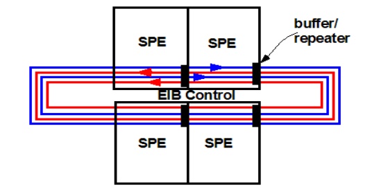
Bus design and communication among the Cell
1: The Element Interconnect Bus:
This bus
makes it possible to link all parts of the chip. The EIB itself is made out of
a 4-ring structure (two clockwise, and two counterclockwise) that is used to
transfer data, and a tree structure used to carry commands. It is actually
controlled by what is called the Data Arbitrer. This structure allows 8
simultaneous transactions on the bus.
2: Input/output interfaces:
The Memory Interface Controller
(MIC).:
Ø It
provides an interface between the EIB and the main storage.
Ø It
currently supports two Rambus Extreme Data Rate (XDR) I/O (XIO) memory
channels.
The Cell Broadband Engine Interface (BEI):
Ø This is
the interface between the Cell and I/O devices,such as GPUs and various
bridges.
Ø It supports
two Rambus FlexIO external I/O channels.
Ø One of
this channel only supports non-coherent transfers. The other supports either
coherent or noncoherenT.
Key Attributes of Cell
Ø Cell is
Multi-Core
Ø Cell is a
Flexible Architecture
Ø Cell is a
Broadband Architecture
Ø Cell is a
Real-Time Architecture
Ø Cell is a
Security Enabled Architecture
Related Topics