Chapter: Digital Electronics : Memory Devices
Programmable Logic Devices - An Overview
Programmable Logic Devices - An Overview
There are many types of programmable logic device, distinguishable from one another in terms of architecture, logic capacity, programmability and certain other specific features. In this section, we will briefly discuss commonly used PLDs and their salient features. A detailed description of each of them will follow in subsequent sections.
1. Programmable ROMs
PROM (Programmable Read Only Memory) and EPROM (Erasable Programmable Read Only Memory) can be considered to be predecessors to PLDs. The architecture of a programmable ROM allows the user to hardware-implement an arbitrary combinational function of a given number of inputs. When used as a memory device, n inputs of the ROM (called address lines in this case) and m outputs (called data lines) can be used to store 2n m-bit words.
When used as a PLD, it can be used to implement m different combinational functions, with each function being a chosen function of n variables. Any conceivable n-variable Boolean function can be made to appear at any of the m output lines. A generalized ROM device with n inputs and m outputs has 2n hard-wired AND gates at the input and m programmable OR gates at the output. Each AND gate has n inputs, and each OR gate has 2n inputs. Thus, each OR gate can be used to generate any conceivable Boolean function of n variables, and this generalized ROM can be used to produce m arbitrary n-variable Boolean functions.
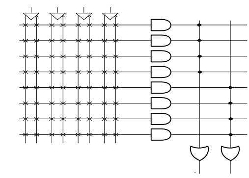
The AND array produces all possible minterms of a given number of input variables, and the programmable OR array allows only the desired minterms to appear at their inputs. Figure shows the internal architecture of a PROM having four input lines, a hard-wired array of 16 AND gates and a programmable array of four OR gates.
A cross (×) indicates an intact (or unprogrammed) fusible link or interconnection, and a dot (•) indicates a hard-wired interconnection. PROMs, EPROMs and EEPROMs (Electrically Erasable Programmable Read Only Memory) can be programmed using standard PROM programmers. One of the major disadvantages of PROMs is their inefficient use of logic capacity. It is not economical to use PROMs for all those applications where only a few minterms are needed.
Other disadvantages include relatively higher power consumption and an inability to provide safe covers for asynchronous logic transitions. They are usually much slower than the dedicated logic circuits. Also, they cannot be used to implement sequential logic owing to the absence of flip-flops.
2. Programmable Logic Array
A programmable logic array (PLA) device has a programmable AND array at the input and a programmable OR array at the output, which makes it one of the most versatile PLDs. Its architecture differs from that of a PROM in the following respects. It has a programmable AND array rather than a hard-wired AND array. The number of AND gates in an m-input PROM is always equal to 2m . In the case of a PLA, the number of AND gates in the programmable AND array for m input variables is usually much less than 2m , and the number of inputs of each of the OR gates equals the number of AND gates. Each OR gate can generate an arbitrary Boolean function with a maximum of minterms equal to the number of AND gates. Figure 9.4 shows the internal architecture of a PLA device with four input lines, a programmable array of eight AND gates at the input and a programmable array of two OR gates at the output. A PLA device makes more efficient use of logic capacity than a PROM. However, it has its own disadvantages resulting from two sets of programmable fuses, which makes it relatively more difficult to manufacture, program and test.
GAL device can be erased and reprogrammed. Also, it has reprogrammable output logic. This feature makes it particularly attractive at the device prototyping stage, as any bugs in the logic can be corrected by reprogramming. A similar device called PEEL (Programmable Electrically Erasable Logic) was introduced by the International CMOS Technology (ICT) Corporation.
3. Complex Programmable Logic Device
Programmable logic devices such as PLAs, PALs, GALs and other PAL-like devices are often grouped into a single category called simple programmable logic devices (SPLDs) to distinguish them from the ones that are far more complex.
A complex programmable logic device (CPLD), as the name suggests, is a much more complex device than any of the programmable logic devices discussed so far. A CPLD may contain circuitry equivalent to that of several PAL devices linked to each other by programmable interconnections. Figure shows the internal structure of a typical CPLD. Each of the four logic blocks is equivalent to a PLD such as a PAL device.
The number of logic blocks in a CPLD could be more or less than four. Each of the logic blocks has programmable interconnections. A switch matrix is used for logic block to logic block interconnections. Also, the switch matrix in a CPLD may or may not be fully connected. That is, some of the possible connections between logic block outputs and inputs may not be supported by a given CPLD.
While the complexity of a typical PAL device may be of the order of a few hundred logic gates, a CPLD may have a complexity equivalent to tens of thousands of logic gates. When compared with FPGAs, CPLDs offer predictable timing characteristics owing to their less flexible internal architecture and are thus ideal for critical control applications and other applications where a high performance level is required. Also, because of their relatively much lower power consumption and lower cost, CPLDs are an ideal solution for battery-operated portable applications such as mobile phones, digital assistants and so on.
A CPLD can be programmed either by using a PAL programmer or by feeding it with a serial data stream from a PC after soldering it on the PC board. A circuit on the CPLD decodes the data stream and configures it to perform the intended logic function.
4. Field-Programmable Gate Array
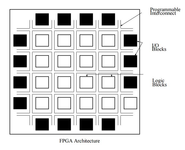
A field-programmable gate array (FPGA) uses an array of logic blocks, which can be configured by the user. The term ‘field-programmable’ here signifies that the device is programmable outside the factory where it is manufactured. The internal architecture of an FPGA device has three main parts, namely the array of logic blocks, the programmable interconnects and the I/O blocks.
Figure shows the architecture of a typical FPGA. Each of the I/O blocks provides an individually selectable input, output or bidirectional access to one of the general-purpose I/O pins on the FPGA package. The logic blocks in an FPGA are no more complex than a couple of logic gates or a look-up table feeding a flip-flop. The programmable interconnects connect logic blocks to logic blocks and also I/O blocks to logic blocks.
FPGAs offer a much higher logic density and much larger performance features compared with CPLDs. Some of the contemporary FPGA devices offer a logic complexity equivalent to that of eight million system gates. Also, these devices offer features such as built-in hard-wired processors,
large memory, clock management systems and support for many of the contemporary device-to- device signalling technologies. FPGAs find extensive use in a variety of applications, which include data processing and storage, digital signal processing, instrumentation and telecommunications
Related Topics