Chapter: Digital Principles and System Design : Combinational Logic
Combinational Logic
COMBINATIONAL LOGIC
Introduction
The term .combinational. comes to us from mathematics. In mathematics a combination is an unordered set, which is a formal way to say that nobody cares which order the items came in. Most games work this way, if you rolled dice one at a time and get a 2 followed by a 3 it is the same as if you had rolled a 3 followed by a 2. With combinational logic, the circuit produces the same output regardless of the order the inputs are changed. There are circuits which depend on the when the inputs change, these circuits are called sequential logic. Even though you will not find the term .sequential logic. in the chapter titles, the next several chapters will discuss sequential logic. Practical circuits will have a mix of combinational and sequential logic, with sequential logic making sure everything happens in order and combinational logic performing functions like arithmetic, logic, or conversion.
1 Design Using Gates
A combinational circuit is one where the output at any time depends only on the present combination of inputs at that point of time with total disregard to the past state of the inputs. The logic gate is the most basic building block of combinational logic. The logical function performed by a combinational circuit is fully defined by a set of Boolean expressions. The other category of logic circuits, called sequential logic circuits, comprises both logic gates and memory elements such as flip-flops. Owing to the presence of memory elements, the output in a sequential circuit depends upon not only the present but also the past state of inputs.
The Fig 3.1 shows the block schematic representation of a generalized combinational circuit having n input variables and m output variables or simply outputs. Since the number of input variables is
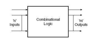
Fig 3.1 Generalized Combinational Circuit
n, there are 2n possible combinations of bits at the input. Each output can be expressed in terms of input variables by a Boolean expression, with the result that the generalized system of above fig can be expressed by m Boolean expressions. As an illustration, Boolean expressions describing the function of a four-input OR/NOR gate are given as
 ….. Eq – 1
2 BCD Arithmetic Circuits
Addition and subtraction are the two most commonly used arithmetic operations, as the other two, namely multiplication and division, are respectively the processes of repeated addition and repeated subtraction, as was outlined in Chapter 2 dealing with binary arithmetic. We will begin with the basic building blocks that form the basis of all hardware used to perform the aforesaid arithmetic operations on binary numbers. These include half-adder, full adder, half-subtractor, full subtractor and controlled inverter.
3 Binary Adder
3.1 Half-Adder
A half-adder is an arithmetic circuit block that can be used to add two bits. Such a circuit thus has two inputs that represent the two bits to be added and two outputs, with one producing the SUM output and the other producing the CARRY. Figure 3.2 shows the truth table of a half-adder, showing all possible input combinations and the corresponding outputs.
The Boolean expressions for the SUM and CARRY outputs are given by the equations below
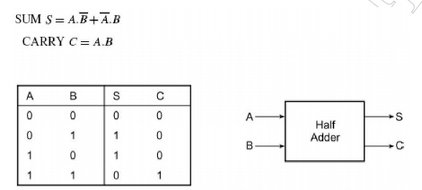
Fig 3.2 Truth Table of Half Adder
An examination of the two expressions tells that there is no scope for further simplification. While the first one representing the SUM output is that of an EX-OR gate, the second one representing the CARRY output is that of an AND gate. However, these two expressions can certainly be represented in different forms using various laws and theorems of Boolean algebra to illustrate the flexibility that the designer has in hardware-implementing as simple a combinational function as that of a half-adder.
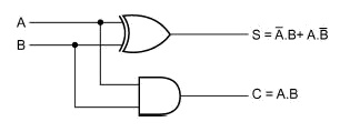
Fig 3.3 Logic Implementation of Half Adder
Although the simplest way to hardware-implement a half-adder would be to use a two-input EX-OR gate for the SUM output and a two-input AND gate for the CARRY output, as shown in Fig. 3.3, it could also be implemented by using an appropriate arrangement of either NAND or NOR gates.
3.2 Full Adder
A full adder circuit is an arithmetic circuit block that can be used to add three bits to produce a SUM and a CARRY output. Such a building block becomes a necessity when it comes to adding binary numbers with a large number of bits. The full adder circuit overcomes the limitation of the half-adder, which can be used to add two bits only. Let us recall the procedure for adding larger binary numbers. We begin with the addition of LSBs of the two numbers. We record the sum under the LSB column and take the carry, if any, forward to the next higher column bits. As a result, when we add the next adjacent higher column bits, we would be required to add three bits if there were a carry from the previous addition. We have a similar situation for the other higher column bits. Also until we reach the MSB. A full adder is therefore essential for the hardware implementation of an adder circuit capable of adding larger binary numbers. A half-adder can be used for addition of LSBs only.
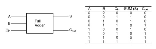
Fig 3.4 Truth Table of Full Adder
Figure 3.4 shows the truth table of a full adder circuit showing all possible input combinations and corresponding outputs. In order to arrive at the logic circuit for hardware implementation of a full adder, we will firstly write the Boolean expressions for the two output variables, that is, the SUM and CARRY outputs, in terms of input variables. These expressions are then simplified by using any of the simplification techniques described in the previous chapter. The Boolean expressions for the two output variables are given in Equation below for the SUM output (S) and in above Equation for the CARRY output (Cout):
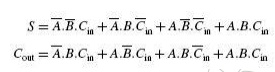
The next step is to simplify the two expressions. We will do so with the help of the Karnaugh mapping technique. Karnaugh maps for the two expressions are given in Fig. 3.5(a) for the SUM output and Fig. 3.5(b) for the CARRY output. As is clear from the two maps, the expression for the SUM (S) output cannot be simplified any further, whereas the simplified Boolean expression for Cout is given by the equation
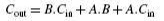
Figure 3.6 shows the logic circuit diagram of the full adder. A full adder can also be seen to comprise two half-adders and an OR gate. The expressions for SUM and CARRY outputs can be rewritten as follows:
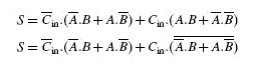
Similarly, the expression for CARRY output can be rewritten as follows:
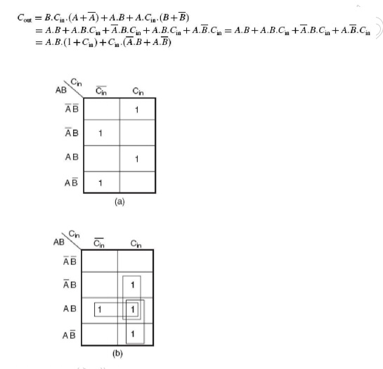
Fig 3.5 Karnaugh Map for the sum and carry out of a full adder
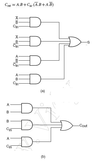
Fig 3.6 Logic circuit diagram of full adder
Boolean expression above can be implemented with a two-input EX-OR gate provided that one of the inputs is Cin and the other input is the output of another two-input EX-OR gate with A and B as its inputs. Similarly, Boolean expression above can be implemented by ORing two minterms. One of them is the AND output of A and B. The other is also the output of an AND gate whose inputs are Cin and the output of an EX-OR operation on A and B. The whole idea of writing the Boolean expressions in this modified form was to demonstrate the use of a half-adder circuit in building a full adder. Figure 3.7(a) shows logic implementation of Equations above. Figure 3.7(b) is nothing but Fig. 3.7(a) redrawn with the portion of the circuit representing a half-adder replaced with a block. The full adder of the type described above forms the basic building block of binary adders. However, a single full adder circuit can be used to add one-bit binary numbers only. A cascade arrangement of these adders can be used to
construct adders capable of adding binary numbers with a larger number of bits. For example, a four-bit binary adder would require four full adders of the type shown in Fig. 3.7 to be connected in cascade. Figure 3.8 shows such an arrangement. (A3A2A1A0) and (B3B2B1B0) are the two binary numbers to be added, with A0 and B0 representing LSBs and A3 and B3 representing MSBs of the two numbers.
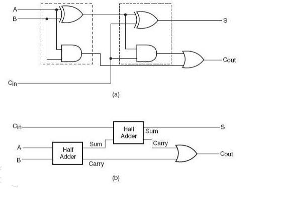
Fig 3.7 Logic Implementation of a full adder with Half Adders
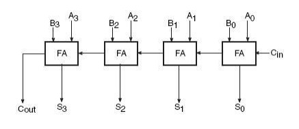
Fig 3.8 Four Bit Binary Adder
4 Half-Subtractor
We will study the use of adder circuits for subtraction operations in the following pages. Before we do that, we will briefly look at the counterparts of half-adder and full adder circuits in the half-subtractor and full subtractor for direct implementation of subtraction operations using logic gates. A half-subtractor is a combinational circuit that can be used to subtract one binary digit from another to produce a DIFFERENCE output and a BORROW output.
The BORROW output here specifies whether a =1‘ has been borrowed to perform the subtraction. The truth table of a half-subtractor, as shown in Fig. 3.9, explains this further. The Boolean expressions for the two outputs are given by the equations
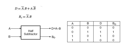
Fig 3.9 Half Subtractor
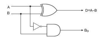
Fig 3.10 Logic Diagram of a Half Subtractor
It is obvious that there is no further scope for any simplification of the Boolean expressions given by above equations. While the expression for the DIFFERENCE (D) output is that of an EX-OR gate, the expression for the BORROW output (Bo) is that of an AND gate with input
A complemented before it is fed to the gate. Figure 3.10 shows the logic implementation of a half-subtractor. Comparing a half-subtractor with a half-adder, we find that the expressions for the SUM and DIFFERENCE outputs are just the same. The expression for BORROW in the case of the half-subtractor is also similar to what we have for CARRY in the case of the half-adder. If the input A, that is, the minuend, is complemented, an AND gate can be used to implement the BORROW output. Note the similarities between the logic diagrams of Fig. 3.3
(half-adder) and Fig. 3.10 (half-subtractor).
4.1 Full Subtractor
A full subtractor performs subtraction operation on two bits, a minuend and a subtrahend, and also takes into consideration whether a =1‘ has already been borrowed by the previous adjacent lower minuend bit or not. As a result, there are three bits to be handled at the input of a full subtractor, namely the two bits to be subtracted and a borrow bit designated as Bin . There are two outputs, namely the DIFFERENCE output D and the BORROW output Bo. The BORROW output bit tells whether the minuend bit needs to borrow a =1‘ from the next possible higher minuend bit. Figure 3.11 shows the truth table of a full subtractor.
The Boolean expressions for the two output variables are given by the equations
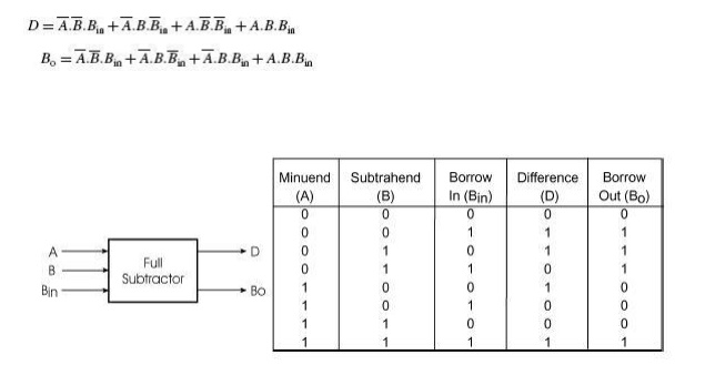
Fig 3.11 Truth Table of Full Subtractor
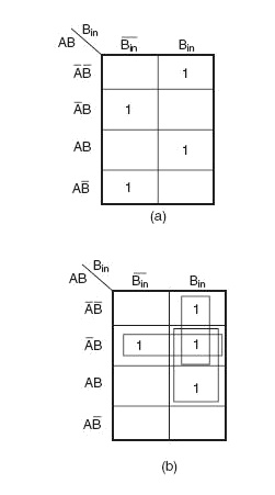
Fig 3.12 K Maps for Difference and Borrow outputs
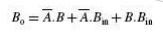
The Karnaugh maps for the two expressions are given in Fig. 3.12(a) for DIFFERENCE output D and in Fig. 3.12(b) for BORROW output Bo. As is clear from the two Karnaugh maps, no simplification is possible for the difference output D. The simplified expression for Bo is given by the equation
If we compare these expressions with those derived earlier in the case of a full adder, we find that the expression for DIFFERENCE output D is the same as that for the SUM output. Also, the expression for BORROW output Bo is similar to the expression for CARRY-OUT Co. In the case of a half-subtractor, the A input is complemented. By a similar analysis it can be shown that a full subtractor can be implemented with half-subtractors in the same way as a full adder was constructed using half-adders. Relevant logic diagrams are shown in Figs 3.7(a) and (b) corresponding to Figs 3.7(a) and (b) respectively for a full adder. Again, more than one full subtractor can be connected in cascade to perform subtraction on two larger binary numbers. As an illustration, Fig. 3.13 shows a four-bit subtractor.
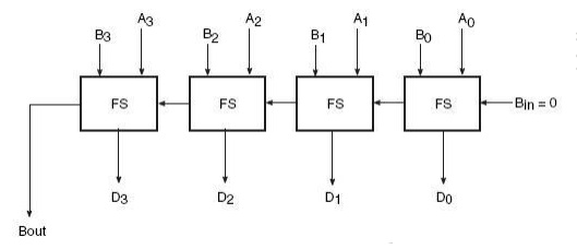
Fig 3.13 Four Bit Subtractor
5 Multipliers
Multiplication of binary numbers is usually implemented in microprocessors and microcomputers by using repeated addition and shift operations. Since the binary adders are designed to add only two binary numbers at a time, instead of adding all the partial products at the end, they are added two at a time and their sum is accumulated in a register called the accumulator register. Also, when the multiplier bit is =0‘, that very partial product is ignored, as an all =0‘ line does not affect the final result. The basic hardware arrangement of such a binary multiplier would comprise shift registers for the multiplicand and multiplier bits, an accumulator register for storing partial products, a binary parallel adder and a clock pulse generator to time various operations.
Binary multipliers are also available in IC form. Some of the popular type numbers in the TTL family include 74261 which is a 2 × 4 bit multiplier (a four-bit multiplicand designated as B0,B1,B2,B3 and B4, and a two-bit multiplier designated as M0, M1 and M2. The MSBs B4 and M2 are used to represent signs. 74284 and 74285 are 4 × 4 bit multipliers. They can be used together to perform high-speed multiplication of two four-bit numbers. Figure 3.14 shows the arrangement. The result of multiplication is often required to be stored in a register. The size of this register (accumulator) depends upon the number of bits in the result, which at the most can be equal to the sum of the number of bits in the multiplier and multiplicand. Some multipliers ICs have an in-built register.
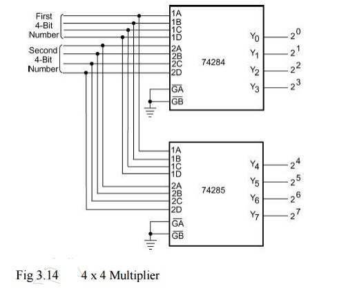
Fig 3.14 4 x 4 Multiplier
Many microprocessors do not have in their ALU the hardware that can perform multiplication or other complex arithmetic operations such as division, determining the square root, trigonometric functions, etc. These operations in these microprocessors are executed through software. For example, a multiplication operation may be accomplished by using a software program that does multiplication through repeated execution of addition and shift instructions. Other complex operations mentioned above can also be executed with similar programs.
Although the use of software reduces the hardware needed in the microprocessor, the computation time in general is higher in the case of software-executed operations when compared with the use of hardware to perform those operations.
HDL (HARDWARE DESCRIPTION LANGUAGE)
In electronics, a hardware description language or HDL is any language from a class of computer languages and/or programming languages for formal description of digital logic and electronic circuits. It can describe the circuit's operation, its design and organization, and tests to verify its operation by means of simulation.
HDLs are standard text-based expressions of the spatial and temporal structure and behaviour of electronic systems. In contrast to a software programming language, HDL syntax and semantics include explicit notations for expressing time and concurrency, which are the primary attributes of hardware. Languages whose only characteristic is to express circuit connectivity between hierarchies of blocks are properly classified as netlist languages used on electric computer-aided design (CAD).
HDLs are used to write executable specifications of some piece of hardware. A simulation program, designed to implement the underlying semantics of the language statements, coupled with simulating the progress of time, provides the hardware designer with the ability to model a piece of hardware before it is created physically. It is this executability that gives HDLs the illusion of being programming languages. Simulators capable of supporting discrete-event (digital) and continuous-time (analog) modeling exist, and HDLs targeted for each are
available.
Design using HDL
The vast majority of modern digital circuit design revolves around an HDL description of the desired circuit, device, or subsystem. Most designs begin as a written set of requirements or a high-level architectural diagram. The process of writing the HDL description is highly dependent on thedesigner's background and the circuit's nature. The HDL is merely the 'capture language'—often begin with a high-level algorithmic description such as MATLAB or a C++ mathematical model. Control and decision structures are often prototyped in flowchart applications, or entered in a state-diagram editor.
Designers even use scripting languages (such as Perl) to automatically generate repetitive circuit structures in the HDL language. Advanced text editors (such as Emacs) offer editor templates for automatic indentation, syntax-dependent coloration, and macro-based expansion of entity/architecture/signal declaration.
As the design's implementation is fleshed out, the HDL code invariably must undergo code review, or auditing. In preparation for synthesis, the HDL description is subject to an array of automated checkers. The checkers enforce standardized code a guideline, identifying ambiguous code constructs before they can cause misinterpretation by downstream synthesis, and check for common logical coding errors, such as dangling ports or shorted outputs.In industry parlance, HDL design generally ends at the synthesis stage. Once the synthesis tool
has mapped the HDL description into a gate netlist, this netlist is passed off to the back-end stage. Depending on the physical technology (FPGA, ASIC gate-array, ASIC standard-cell), HDLs may or may not play a significant role in the back-end flow. In general, as the design flow progresses toward a physically realizable form, the design database becomes progressively more laden with technology-specific information, which cannot be stored in a generic HDL-description. Finally, a silicon chip is manufactured in a fab.
HDL and programming languages
A HDL is analogous to a software programming language, but with major differences. Programming languages are inherently procedural (single-threaded), with limited syntactical and semantic support to handle concurrency. HDLs, on the other hand, can model multiple parallel processes (such as flipflops, adders, etc.) that automatically execute independently of one another. Any change to the process's input automatically triggers an update in the simulator's process stack. Both programming languages and HDLs are processed by a compiler (usually called a synthesizer in the HDL case), but with different goals. For HDLs, 'compiler' refers to synthesis, a process of transforming the HDL code listing into a physically realizable gate netlist. The netlist output can take any of many forms: a "simulation" netlist with gate-delay information, a "handoff" netlist for post-synthesis place and route, or a generic industry-standard EDIF format (for subsequent conversion to a JEDEC-format file). On the other hand, a software compiler converts the source-code listing into a microprocessor-specific object-code, for execution on the target microprocessor. As HDLs and programming languages borrow concepts and features from each other, the boundary between them is becoming less distinct. However, pure HDLs are unsuitable for general purpose software application development, just as general-purpose programming languages are undesirable for modeling hardware. Yet as electronic systems grow increasingly complex, and reconfigurable systems become increasingly mainstream, there is growing desire in the industry for a single language that can perform some tasks of both hardware design and software programming. SystemC is an example of such—embedded system hardware can be modeled as non-detailed architectural blocks (blackboxes with modeled signal inputs and output drivers). The target application is written in C/C++, and natively compiled for the host-development system (as opposed to targeting the embedded CPU, which requires host-simulation of the embedded CPU). The high level of abstraction of SystemC models is well suited to early architecture exploration, as architectural modifications can be easily evaluated with little concern for signal-level implementation issues. In an attempt to reduce the complexity of designing in HDLs, which have been compared to the equivalent of assembly languages, there are moves to raise the abstraction level of the design. Companies such as Cadence, Synopsys and AgilityDesign Solutions are promoting SystemC as a way to combine high level languages with concurrency models to allow faster design cycles for FPGAs than is possible using traditional HDLs. Approaches based on standard C or C++ (with libraries or other extensions allowing parallel programming) are found in the Catapult C tools from Mentor Graphics, and in the Impulse C tools from Impulse Accelerated Technologies. Annapolis Micro Systems, Inc.'s CoreFire Design Suite and National Instruments LabVIEW FPGA provide a graphical dataflow approace to high-level design entry. Languages such as SystemVerilog, SystemVHDL, and Handel-C seek to accomplish the same goal, but are aimed at making existing hardware engineers more productive versus making FPGAs more accessible to existing software engineers. Thus SystemVerilog is more quickly and widely adopted than SystemC. There is more information on C to HDL and Flow to HDL in their respective articles.
Related Topics