Chapter: High Voltage Engineering : Measurement of High Voltage and High Currents
Capacitance Potential Dividers - Digital Techniques in High Voltage Measurement
Capacitance Potential Dividers
Capacitance
potential dividers are more complex than the resistance type. For measurement
of impulse voltages not exceeding 1 MV capacitance dividers can be both
portable and transportable. In general, for measurement of 1 MV and over, the
capacitance divider is a laboratory fixture. The capacitance dividers are
usually made of capacitor units mounted one above the other and bolted
together. It is this failure which makes the small dividers portable. A
screening box similar to that described earlier can be used for housing both
the low voltage capacitor unit C2 and the matching resistor if
required.
The low
voltage capacitor C2 should be non-inductive. A form of capacitor
which has given excellent results is of mica and tin foil plate, construction,
each foil having connecting tags coming out at opposite corners. This ensures
that the current cannot pass from the high voltage circuit to the delay cable
without actually going through the foil electrodes. It is also important that
the coupling between the high and low voltage arms of the divider be purely
capacitive. Hence, the low voltage arm should contain one capacitor only; two
or more capacitors in parallel must be avoided because of appreciable
inductance that would thus be introduced. Further, the tappings to the delay
cable must be taken off as close as possible to the terminals of C2.
Fig. 4.21 shows variants of capacitance potential dividers.
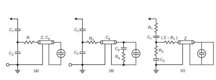
Figure:
4.13 Capacitor dividers (a) Simple matching (b) Compensated matching(c) Damped
capacitor divider simple matching For voltage dividers in FIG. (b) and (c), the
delay cable cannot be matched at its end.
A low
Resistor in parallel to C2 would load the low voltage arm of the
divider too heavily and decrease the output voltage with time. Since R and Z
form a potential divider and R = Z, the voltage input to the cable will be half
of the voltage across the capacitor C2. This halved voltages travels
towards the open end of the cable (CRO end) and gets doubled after reflection.
That is, the voltage recorded by the CRO is equal to the voltage across the
capacitor C2. The reflected wave charges the cable to its final
voltage magnitude and is absorbed by R (i.e. reflection takes place at R and
since R = Z, the wave is completely absorbed as coefficient of voltage
reflection is zero) as the capacitor C2 acts as a short circuit for high
frequency waves. The transformation ratio, therefore, changes from the value:
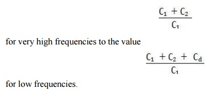
However,
the capacitance of the delay cable Cd is usually small as compared with C2.For
capacitive divider an additional damping resistance is usually connected in the
lead on the High voltage side as shown in FIG. 4.14 (c). The performance of the
divider can be improved if damping resistor which corresponds to the a periodic
limiting case is inserted in series with the individual element of capacitor
divider. This kind of damped capacitive divider acts for high frequencies as a
resistive divider and for low frequencies as a capacitive divider. It can,
therefore, be used over a wide range of frequencies i.e. for impulse voltages
of very different duration and also for alternating voltages.
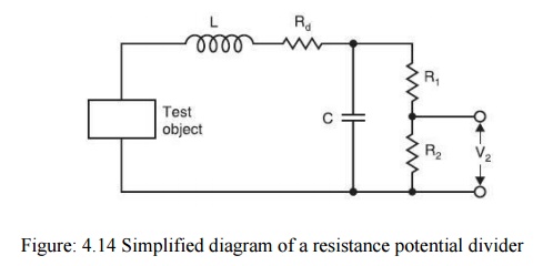
Fig. 4.22
shows a simplified diagram of a resistance potential divider after taking into
Considerations the lead in connection as the inductance and the stray
capacitance as lumped capacitance. Here L represents the loop inductance of the
lead-in connection for the high voltage arm. The damping resistance Rd limits
the transient overshoot in the circuit formed by test object, L, Rd and C. Its
value has a decided effect on the performance of the divider. In order to
evaluate the voltage transformation of the divider, the low voltage arm voltage
V2 resulting from a square wave impulse V1 on the hv side
must be investigated. The voltage V2 follows curve 2 in Fig. 4.15
(a) in case of a periodic damping and curve 2in Fig. 4.15 (b) in case of
sub-critical damping. The total area between curves 1 and 2 taking into
consideration the polarity is described as the response time.
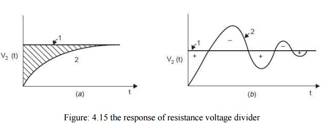
With
subcritical damping, even though the response time is smaller, the damping
should not be Very small. This is because an undesirable resonance may occur
for a certain frequency within the passing frequency band of the divider. A
compromise must therefore be realized between the short rise time and the rapid
stabilization of the measuring system. According to IEC publication No. 60 a
maximum overshoot of 3% is allowed for the full impulse wave, 5% for an impulse
wave chopped on the front at times shorter than 1 micro sec. In order to
fulfill these requirements, the response time of the divider must not exceed
0.2 micro sec. for full impulse waves 1.2/50 or 1.2/5 or impulse waves chopped
on the tail. If the impulse wave is chopped on the front at time shorter than 1
micro sec the response time must be not greater than 5% of the time to
chopping.
Related Topics