Chapter: Electronic Devices : Semiconductor Diode
Quantitative Theory of P-N Diode Currents
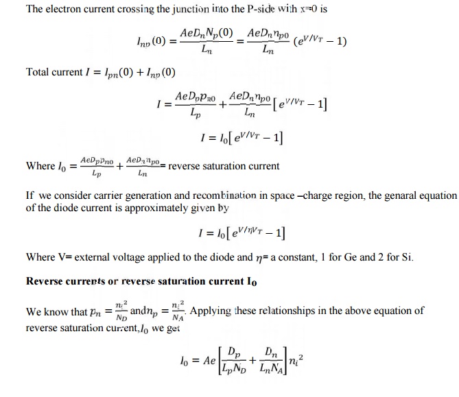
QUANTITATIVE THEORY OF P-N DIODE CURRENTS
To derive the expression for the total current as function of applie d voltage (neglect the barrier width)When diode is fo rward biased, holes injected from the p to n material. The concentration pn of holes in the n-side is increased above equilibrium value pno is the diffusion length for holes in the N-material and the injected or excess concentration at x=0 is
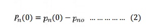
Equation (2) shows the exponential decrease of density pn(x) with distance x into the N-material.
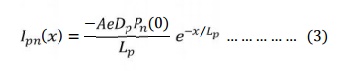
From equation 3 hole current decreases exponentially with distance. It is depending on Pn(0) , because it is a function of applied voltage. Ipn depends on applied voltage or injected concentration is a function of voltage.
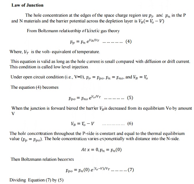
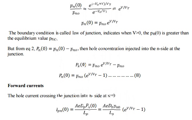
Law of Junction
1 DIODE CURRENT EQUATION
The diode current equation relating the voltage V and current I is given by
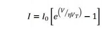
where
I – diode current
Io – diode reverse saturation current at room temperature
V – External voltage applied to the diode
η - a constant, 1 for Ge and 2 for Si VT = kT/q = T/11600, thermal voltage
K – Boltzmann‘s constant (1.38066x10^-23 J/K) q – Charge of electron (1.6x10^-19 C)
T – Temperature of the diode junction
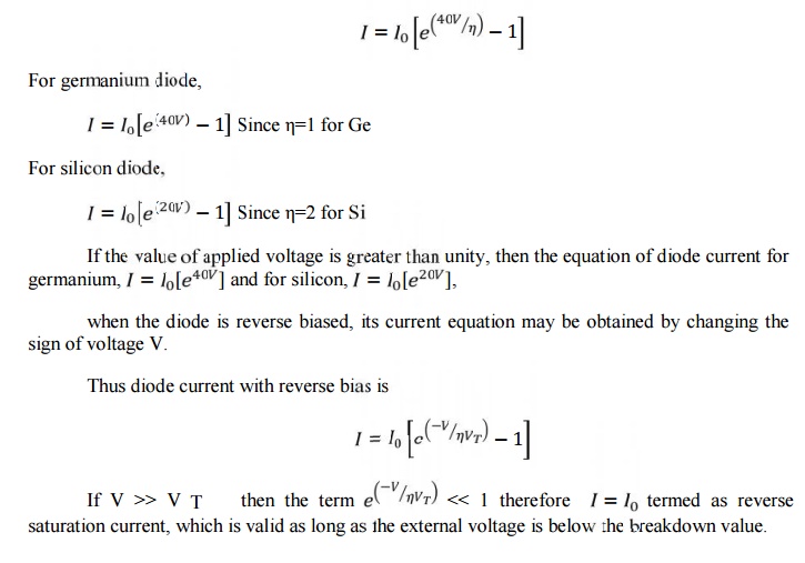
At room temperature (T=300 K), VT = 26mV. Substituting this value in current equation,
DRIFT AND DIFFUSION CURRENTS
· The flow of charge (ie) current through a semiconductor material are of two types namely drift & diffusion. (ie) The net current that flows through a (PN junction diode) semiconductor material has two components
(i) Drift current (ii) Diffusion current
1 DRIFT CURRENT
· When an electric field is applied across the semiconductor material, the charge carriers attain a certain drift velocity Vd , which is equal to the product of the mobility of the charge carriers and the applied Electric Field intensity E .
Drift velocity Vd = mobility of the charge carriers X Applied Electric field intensity.
· Holes move towards the negative terminal of the battery and electrons move towards the positive terminal of the battery. This combined effect of movement of the charge carriers constitutes a current known as ― the drift current.
· Thus the drift current is defined as the flow of electric current due to the motion of the charge carriers under the influence of an external electric field.
· Drift current due to the charge carriers such as free electrons and holes are the current passing through a square centimeter perpendicular to the direction of flow.
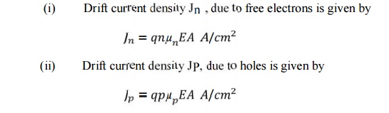
Where, n - Number of free electrons per cubic centimetre.
P - Number of holes per cubic centimetre
μ(n) – Mobility of electrons in cm2 / Vs
μ (p) – Mobility of holes in cm2 / Vs
E – Applied Electric filed Intensity in V /cm
q – Charge of an electron = 1.6 x 10⁻¹⁹ coulomb.
2 DIFFUSION CURRENT
· It is possible for an electric current to flow in a semiconductor even in the absence of the applied voltage provided a concentration gradient exists in the material.
· A concentration gradient exists if the number of either elements or holes is greater in one region of a semiconductor as compared to the rest of the Region.
Figure 1.4 (a) Exess hole concentration varying along the axis in an N-type semiconductor bar, (b) The resulting diffusion current
→ In a semiconductor material the change carriers have the tendency to move from the region of higher concentration to that of lower concentration of the same type of charge carriers.
Thus the movement of charge carriers takes place resulting in a current called diffusion current.
As indicated in fig a, the hole concentration p(x) in semiconductor bar varies from a high value to a low value along the x-axis and is constant in the y and z directions.
Diffusion current density due to holes Jp is given by
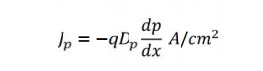
Since the hole density p(x) decreases with increasing x as shown in fig b, dp/dx is negative and the minus sign in equation is needed in order that Jp has positive sign in the positive x direction.
Diffusion current density due to the free electrons is given by
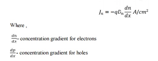
Dn and Dp – diffusion coefficient for electrons and holes
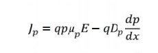
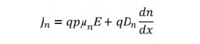
Total Current
The total current in a semiconductor is the sum of both drift and diffusion currents that is given by
Related Topics