Chapter: Electronic Devices : Semiconductor Diode
Important Questions and Answers: Semiconductor Diode
1. Give the value of Charge, Mass of an electron.
Charge of
an electron – 1.6 x 10 -19 coloumbs. Mass of an electron - 9.11 x 10 -31 Kgs
2. Define Potential.
A potential of V volts at point B with respect to
point A, is defined as the work done in taking unit positive charge from A to B
, against the electric field.
3. Define Current density.
It is
defined as the current per unit area of the conducting medium. J = I / A
4. Define Electron volts.
If an electron falls through a potential of one
volt then its energy is 1 electron volt. 1 eV = 1.6 x 10 -19 joules
5. What is atomic number?
The
number of protons or electrons in an atom is atomic number.
6. What are valence electrons?
Electron
in the outermost shell of an atom is called valence electron.
7. What is forbidden energy gap?
The space
between the valence and conduction band is said to be forbidden energy gap.
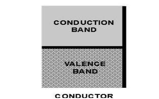
8. What are conductors? Give examples?
Conductors are materials in which the valence and conduction band
overlap each other so there is a swift movement of electrons which leads to
conduction. Ex: Copper, silver.
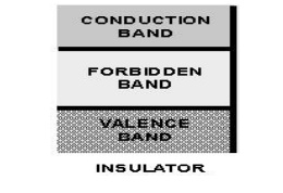
9. What are insulators? Give examples?
Insulators are materials in which the valence and conduction band are
far away from each other. So no movement of free electrons and thus no
conduction. Ex glass, plastic.
10.
What are
Semiconductors? Give examples?
The
materials whose electrical property lies between those of conductors and
insulators are known as Semiconductors. Ex germanium, silicon.
11.
Give the
energy band structure of Insulator.
In Insulators there is a wide forbidden energy gap. So movement of
valence electron from valence to conduction band is not possible.
12.
Give the
energy band structure of Semi conductor.
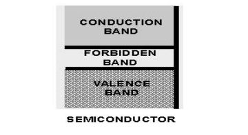
In
Semiconductors th ere is a small forbidden energy gap. So movement of valence
electron from valence to conduction band is possible if the valence electrons
are supplied with some energy.
13.
Give the
energy band structure of conductor.
In conductors there i s no forbidden energy gap, valence band and
conduction and overlap each other. so there is a heavy movement of valence
electrons.
14.
What are
the types o f Semiconductor?
1.
Intrinsic semiconductor 2. Extrinsic semiconductor.
15.
What is
Intrinsic Sem iconductor?
Pure form
of semiconnductors are said to be intrinsic semiconductor. Ex: germanium,
silicon.
16.
What is
Extrinsic Se miconductor?
If certain amount of i mpurity atom is added to
intrinsic semiconduuctor the resulting semiconductor is Extrinsic or impure
Semiconductor.
17. Define Mass – action law.
Under
thermal equili brium the product of free electron concentr ation (n) and hole
concentration (p) is constant regardless of the individual magnitude.
n.p = ni2
18.
What are
the types of Extrinsic Semiconductor?
1.P-type
Semiconductor 2. N- Type Semiconductor.
19.
What is
P-type Semiconductor?
The
Semiconductor which are obtained by introducing pentavalent impurity atom
(phosphorous, antimony) are known as P-type Semiconductor.
20.
What is
N-type Semiconductor?
The
Semiconductor which is obtained by introducing trivalent impurity atom
(gallium, indium) are known as N-type Semiconductor.
21.
What is
doping?
Process
of adding impurity to a intrinsic semiconductor atom is doping. The impurity is
called dopant.
22.
Which
charge carriers is majority and minority carrier in N-type Semiconductor?
Majority
carrier: electron and minority carrier: holes.
23.
Which
charge carriers is majority and minority carrier in P-type Semiconductor?
Majority
carrier: holes and minority carrier: electron
24.
Why n -
type or penta valent impurities are called as Donor impurities?
n- type impurities will donate the excess negative
charge carriers ( Electrons) and therefore they are reffered to as donor
impurities.
25. Why P – type or trivalent
impurities are called as acceptor impurity?
p- type impurities make available positive carriers
because they create holes which can accept electron, so these impurities are
said to be as acceptor impurity.
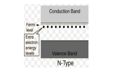
26. Give the energy band structure of n- type
semiconductor.
27. Define drift current?
When an electric field is applied across the semiconductor, the holes
move towards the negative terminal of the battery and electron move towards the
positive terminal of the battery. This drift movement of charge carriers will
result in a current termed as drift current.
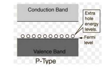
28. Give the energy band structure of P- type
semiconductor.
29. Give the expression for the Fermi level energy
in n – type semiconductor.

Where,
EF - Fermi level energy
EC –
Conduction band energy
K –
Boltzmann constant
T –
Temperature
NC –
dimension of concentration in n – type
ND -
concentration of donor atoms
30. Give the expression for drift current density=µ
due to electron.

31. Give the expression for drift current density=µdue to
holes.

32. Define the term diffusion current?
A
concentration gradient exists, if the number of either electrons or holes is
greater in one region of a semiconductor as compared to the rest of the region.
The holes and electron tend to move from region of higher concentration to the
region of lower concentration. This process in called diffusion and the current
produced due this movement is diffusion current.
33. Give the expression for diffusion current=
density due to electron.

Where
Jn -
diffusion current density due to electron
q -
Charge of an electron
Dn –
diffusion constant for electron
dn / dx –
concentration gradient
34. Give the expression for diffusion current =
density due to holes.

Where
Jp -
diffusion current density due to holes
q -
Charge of a hole Dp – diffusion constant for hole
dn / dx –
concentration gradient
33.
What is
the other name of continuity equation? What does it indicate?
The other
name of continuity equation is equation of conservation of charge.This equation
indicates that the rate at which holes are generated thermally just equals the
rate at which holes are lost because of recombination under equilibrium
conditions.
34.
Define
Hall effect?
If a
metal or semiconductor carrying current I is placed in a transverse magnetic
field B , an electric field E is induced in the direction perpendicular to both
I and B , This phenomenon is known as Hall effect.
35.
Give some
application of Hall Effect.
i.
hall effect can be used to measure the strength of
a magnetic field in terms of electrical voltage.
ii.
it is used to determine whether the semiconductor
is p – type or n- type material
iii.
it is used to determine the carrier concentration
iv.
it is used to determine the mobility.
36.
What is
depletion region in PN junction?
The
region around the junction from which the mobile charge carriers ( electrons
and holes) are depleted is called as depletion region.since this region has
immobile ions, which are electrically charged , the depletion region is also
known as space charge region.
37.
Give the
other names of depletion region? i.space charge region
ii.Transition
region
38.
What is
barrier potential?
Because of the oppositely charged ions present on both sides of PN
junction an electric potential is established across the junction even without
any external voltage source which is termed as barrier potential.
39.
Give the
other names of depletion region? i.space charge region
ii.Transition
region
40.
What is
barrier potential?
Because
of the oppositely charged ions present on both sides of PN junction an electric
potential is established across the junction even without any external voltage
source which is termed as barrier potential.![]()
![]()
![]()

41.
What is
meant by biasing a PN junction?
Connecting
a PN junction to an external voltage source is biasing a PN junction.
42.
What is
forward bias and reverse bias in a PN junction?
When
positive terminal of the external supply is connected to P region and negative
terminal to N region ,the PN junction is said to be forward biased. under
forward biased condition the PN region offers a very low resistance and a large
amount of current flows through it.
43.
What is
reverse bias in a PN junction?
When
positive terminal of the external supply is connected to N type and negative
terminal to P type then the PN junction is said to be in reverse bias. Under
reverse biased condition the PN region offers a very high resistance and a
small amount of current flows through it.
44.
What is
Reverse saturation current?
The
current due to the minority carriers in reverse bias is said to be reverse
saturation current. This current is independent of the value of the reverse
bias voltage.
45.Why a contact difference of potential exist in
PN junction?
When a pn
junction is formed by placing a p-type and n-type material in intimate contact,
the Fermi level throughout the newly formed specimen is not constant at equilibrium.
There will be transfer of electron and energy until Fermi levels in the two
side did line up. But the valence and conduction band in pside cannot be at the
at the same level as in n side .this shift in energy level results in contact
difference of potential.
46. Give the expression of contact difference= of
potential?

Where, E0 - contact difference of potential,
K –
Boltzmann constant ,
T –
Temperature
ND -
concentration of donor atoms ,
NA -
concentration of acceptor atoms
ni –
intrinsic concentration
47. Give the diode current equation?
The diode
current equation relating =the voltage V and−1current I is given by I – diode
current, Io – diode reverse saturation current at room temperature

V –
External voltage applied to the diode, η - a constant, 1 for Ge and 2 for Si
VT = kT/q = T/11600, thermal voltage,
K –
Boltzmann‘s constant (1.38066x10^-23 J/K)
q –
Charge of electron (1.6x10^-19 C)
T –
Temperature of the diode junction
INTRODUCTION
ELECTRON
It is a stable elementary particle with a charge of negative
electricity, found in all atoms and acting as the primary carrier of
electricity in solids.
ELECTRONICS
·
Electronics is the movement of electrons in a
vacuum, gas, semiconductor, etc., in devices in which the flow is controlled
and utilized.
·
Electronics deals with electrical circuits that
involve active electrical components such as vacuum tubes, transistors, diodes
and integrated circuits, and associated passive interconnection technologies.
ELECTRON DEVICES
·
An electronic component is any physical entity in
an electronic system used to affect the electrons or their associated fields in
a manner consistent with the intended function of the electronic system.
·
Components are generally intended to be connected
together, usually by being soldered to a printed circuit board (PCB), to create
an electronic circuit with a particular function (for example an amplifier,
radio receiver, or oscillator). Components may be packaged singly, or in more
complex groups as integrated circuits.
·
Some common electronic components are capacitors,
inductors, resistors, diodes, transistors, etc. Components are often
categorized as active (e.g. transistors and thyristors) or passive (e.g.
resistors and capacitors).
ELECTRONIC CIRCUITS
Circuits
and components can be divided into two groups: Analog and Digital. A particular
device may consist of circuitry that has one or the other or a mix of the two
types.
Analog circuits are constructed from combinations of a few types of
basic circuits. Analog circuits use a continuous range of voltage as opposed to
discrete levels as in digital circuits. The number of different analog circuits
so far devised is huge, especially because a 'circuit' can be defined as
anything from a single component, to systems containing thousands of
components.
Digital circuits are electric circuits based on a number of discrete
voltage levels. Digital circuits are the most common physical representation of
Boolean algebra, and are the basis of all digital computers. To most engineers,
the terms "digital circuit", "digital system" and
"logic" are interchangeable in the context of digital circuits.
Related Topics