Chapter: Electronic Devices : Bipolar Junction
Bipolar Junction
BIPOLAR JUNCTION
1 Introduction transistors and its types
2 NPN -PNP -Junctions and operation
3 Current equations
4 Early effect
5 Input and Output characteristics of CE, CB CC
6 Hybrid -π model
7 h-parameter model
8 Ebers Moll Model
9 Gummel Poon-model
10 Multi Emitter Transistor
1 INTRODUCTION
The transistor is the main building block “element” of electronics. It is a semiconductor device and it comes in two general types: the Bipolar Junction Transistor (BJT) and the Field Effect Transistor (FET).
It is named as transistor which is an acronym of two terms: “transfer-of-resistor.” It means that the internal resistance of transistor transfers from one value to another values depending on the biasing voltage applied to the transistor. Thus it is called TRANSfer resISTOR: i.e.
TRANSISTOR.
A bipolar transistor (BJT) is a three terminal semiconductor device in which the operation depends on the interaction of both majority and minority carriers and hence the name bipolar.
The voltage between two terminals controls the current through the third terminal. So it is called current controlled device. This is the basic principle of the BJT
It can be used as amplifier and logic switches. BJT consists of three terminals:
· Collector : C
· Base : B
· Emitter : E
TYPES
There are two types of bipolar transistors
· NPN transistor and
· PNP transistor.
TRANSISTOR CONSTRUCTION
PNP Transistor: In PNP transistor a thin layer of N-type silicon is sandwiched between two layers of P-type silicon.
NPN Transistor: In NPN transistor a thin layer of P-type silicon is sandwiched between two layers of N-type silicon. The two types of BJT are represented in figure 2.1
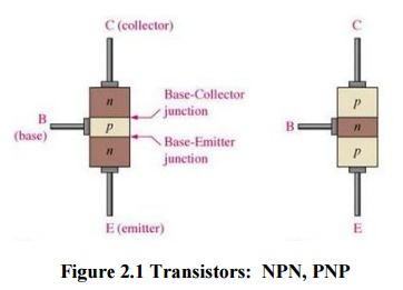
Figure 2.1 Transistors: NPN, PNP
The symbolic representation o f the two types of the BJT is shown in figure 2.2
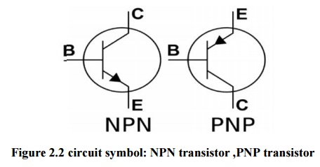
Figure 2.2 circuit symbol: NPN transistor ,PNP trans istor
Area:[C>E>B]
· The area of collector la yer is largest. So it can dissipate heat quickly.
· Area of base layer is sm allest and it is very thin layer.
· Area of emitter layer is medium.
Doping level:[E>C>B]
· Collector layer is moderately doped. So it has medium number of charges.
· Base layer is lightly do ped. So it has a very few number of charges.
· Emitter layer is heavily doped. So it has largest number of charges.
Junctions:
· There are two junctions in this transistor – junction J-1 and junction J-2.
· The junction between collector layer and base layer is called as collector-base junction or C-B junction.
· The junction between base layer and emitter layer is called a s base-emitter junction or B-E junction. The t wo junctions have almost same potential ba rrier voltage of 0.6V to 0.7V, just like in a diode.
Equivalent diode representation:
· The transistor formed by back to back connection of two diodes.
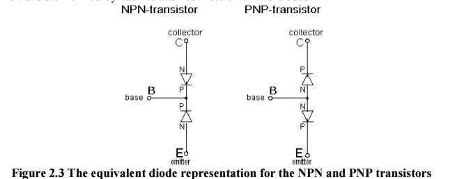
Figure 2.3 The equivalent diode representation for the NPN a nd PNP transistors
TRANSISTOR BIASING
The states of the two pn junctions can be altered by the external circuitry connected to the transistor. This is called biasing the transistor.
Usually the emitter- base junction is forward biased and collector –base junction is reverse biased. Due to forward bias on the emitter- base junction an emitter current flows through the base into the collector. Though, the collector –base junction is reverse biased, almost the entire emitter current flows through the collector circuit.
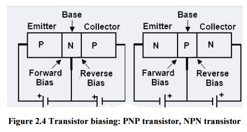
Figure 2.4 Transistor biasing: PNP transistor, NPN transistor
A single pn junction has two different types of bias:
· Forward bias
· Reverse bias
There are two junctions in bipolar junction transistor. Each junction can be forward or reverse biased independently. Thus there are four modes of operations:
Table 2.1 Modes of operation of transistor
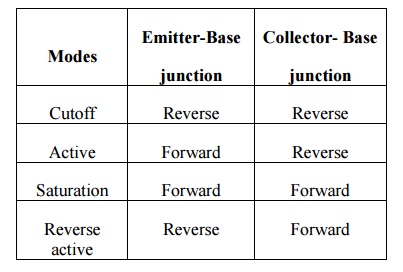
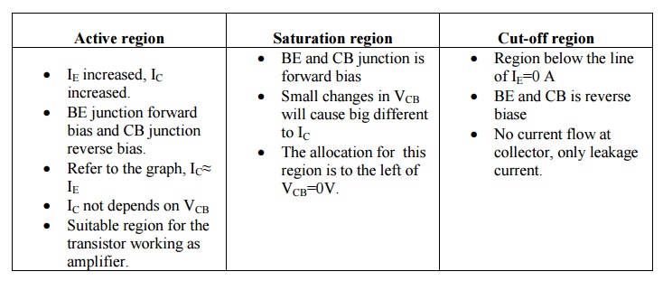
Forward Active
In this mode of operation, emitter-base junction is forward biased and collector base junction is reverse biased. Transistor behaves as a source. With controlled source characteristics the BJT can be used as an amplifier and in analog circuits.
Cut off
When both junctions are rever se biased it is called cut off mode. In this situation there is nearly zero current and transistor behaves as an open switch.
Saturation
In saturation mode both junctions are forward biased large collector current flows with a small voltage across collector base junction. Transistor behaves as an closed switch.
Reverse Active
It is opposite to forward active mode because in this emitter base junction is reverse biased and collector base junction is forward biased. It is called inverted mode. It is no suitable for amplification. However the re verse active mode has application in digi tal circuits and certain analog switching circuits.
TRANSISTOR CURRENTS
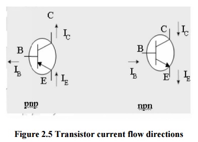
Figure 2.5 Transistor current flow directions
- The arrow is always drawn o n the emitter The arrow always point toward the n-type
- The arrow indicates the dire ction of the emitter current:
pnp:E-> B
npn: B-> E
IC = the collector current, IB = the base current, IE = the emitter current
OPERATION OF AN NPN TRANSISTOR
Emitter base junction is forward biased and collector base junction is reverse biased. Due to emitter base junction is forwar d biased lot of electrons from emitter entering the base region.
Base is lightly doped with P-type impurity. So the number of holes i n the base region is very
small.
Due to this, electron- hole re combination is less (i.e,) few electrons(<5%) combine with holes to constitute base current(IB)
The remaining electrons (>95%) crossover into collector region, to constitute collector current(IC).
Figure 2.6 Current in NPN transistor
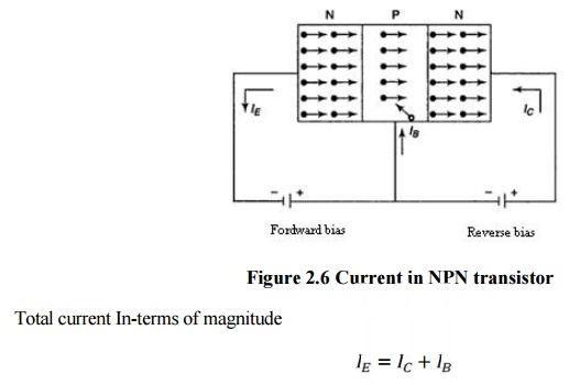
Total current In-terms of magnitude
OPERATION OF A PNP
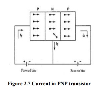
Figure 2.7 Current in PNP transistor
Emitter base junction is forward biased and collector base junction is reverse biased. Due to emitter base junction is forward biased lot of holes from emitter entering the base region and electrons from base to emitter region.
Base is lightly doped with N-type impurity. So the number of electrons in the base region is very small.
Due to this, electron- hole recombination is less (i.e,) few holes (<5%) combine with electrons to constitute base current(IB)
The remaining holes (>95%) crossover into collector region to constitute collector current(IC). Applying KCL to the transistor, the total current =in terms+ of magnitude

CURRENT EQUATIONS
Let‘s consider the BJT npn structure shown on Figure 2.8
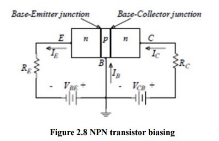
Figure 2.8 NPN transistor biasing
With the voltage VBE and VCB as shown, the Base-Emitter (B-E) junction is forward biased and the Base Collector (B-C) junction is reverse biased.
The current through the B-E junction is related to the B-E voltage as
Due to the large differences in the doping concentrations of the emitter and the base regions the electrons injected into the base region (from the emitter region) results in the emitter current .
Further more the number of electrons injected into the collector region is directly related to the electrons injected into the base region from the emitter region.
Therefore, the collector current is related to the emitter current which is in turn a function of the B-E voltage.
The collector current and the base current=are related
EARLY EFFECT OR BASE WIDTH MODULATION
The early effect is the variation in the width of the base in a bipolar transistor due to a variation in the applied base-to-collector voltage. For example a greater reverse bias across the collector –base junction increases the collector-base depletion width. If VCE increases VCB increases too.
The decrease in the base width by VCB has the following two consequences that affect the current:
· There is a lesser chance for recombination within the "smaller" base region.
· The charge gradient is increased across the base, and consequently, the current of minority carriers injected across the emitter junction increases.
· Punch through (or) Reach through:For extremely large reverse voltage is applied to the C-B junction, the “base width” is reduced to zero, causing voltage breakdown in a transistor. It is known as punch trough or reach through
Both these factors increase the collector or "output" current of the transistor with an increase in the collector voltage. This increased current is shown in Figure 2.9 Tangents to the characteristics at large voltages extrapolate backward to intercept the voltage axis at a voltage called the Early voltage, often denoted by the symbol VA.
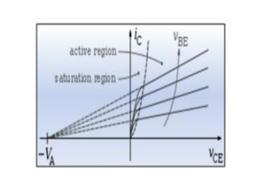
Figure 2.9 Collector current increase with an increase of the collector-emitter voltage due to the Early effect. The Early voltage, VA, is also indicated on the figure.
5 CONFIGURATION OF TRANSISTOR CIRCUIT
A transistor is a three terminal device. But require ‘4’ terminals for connecting it in a circuits.
(i.e.) 2 terminals for input, 2 terminals for output.
Hence one of the terminal is made common to the input and output circuits. Common terminal is grounded.
TYPES OF CONFIGURATIONS
Three types of configuration is available
1) Common base(CB) configuration
2) Common emitter (CE) configuration
3) Common collector (CC) configuration
1 COMMON BASE(CB) CONFIGURATION
In common base configuration circuit is shown in figure. Here base is grounded and it is used as the common terminal for both input and output.
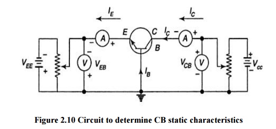
Figure 2.10 Circuit to determine CB static characteristics
It is also called as grounded base configuration. Emitter is used as a input terminal where as collector is the output terminal.
Input characteristics:
It is defined as the characteristic curve drawn between input voltage to input current whereas output voltage is constant.
To determine input characteristics, the collector base voltage VCB is kept constant at zero and emitter current IE is increased from zero by increasing VEB. This is repeated for higher fixed values of VCB.
A curve is drawn between emitter current and emitter base voltage at constant collector base voltage is shown in figure 2.11.When VsCB is zero EB junctions is forward biased. So it behaves as a diode so that emitter current increases rapidly.
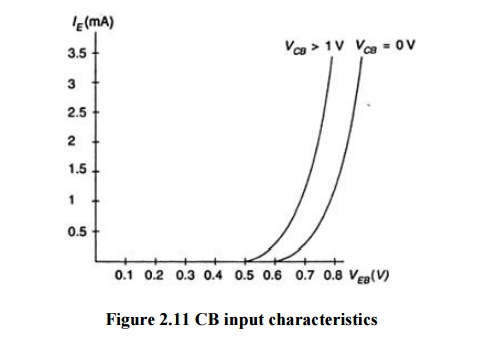
Figure 2.11 CB input characteristics
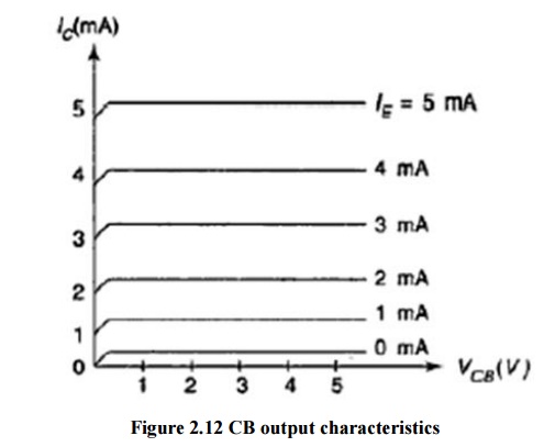
Output Characteristics
It is defined as the characteristic curve drawn between output voltage to output current whereas input current is constant.To determine output characteristics, the emitter current IE is kept constant at zero and collector current Ic is increased from zero by increasing VCB.This is repeated for higher fixed values of IE.
From the characteristic it is seen that for a constant value of IE, Ic is independent of VCB and the curves are parallel to the axis of VCB. As the emitter base junction is forward biased the majority carriers that is electrons from the emitter region are injected into the base region.
In CB configuration a variation of the base-collector voltage results in a variation of the quasi-neutral width in the base. The gradient of the minority-carrier density in the base therefore changes, yielding an increased collector current as the collector-base current is increased. This effect is referred to as the Early effect.
Transistor parameters in CB configuration
The slope of CB characteristics will give the following four transistor parameters. It is known as base hybrid parameters.
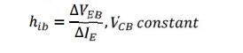
I. Input impedance (hib): It is defined as the ratio of change in input voltage (emitter voltage) to change in input∆current (emitter current) with the output voltage (collector voltage) is kept constantℎ=. ∆ ,
This ranges from 20ohms to 50ohms.
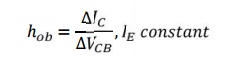
II. Output admittance (hob): It is defined as the ratio of change in output current (collector current) to change in output ∆voltage (collector voltage) with the input current (emitter current) is kept constant ℎ. = ∆ ,
This ranges from 0.1 to 10µ mhos.
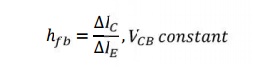
III. Forward current gain (hfb): It is defined as the ratio of change in output current (collector current) to change in input current (emitter current) with the output voltage
(collector voltage) is kept constant∆.
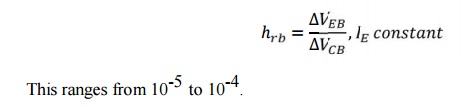
IV. Reverse voltage gain (hrb): It is defined as the ratio of change in input voltage (emitter voltage) to change in output voltage (collector voltage) with the input current (emitter current) is kept constant. ∆
2 CE CONFIGURATION
In common emitter configuration circuit is shown in figure. Here emitter is grounded and it is used as the common terminal for both input and output. It is also called as grounded emitter configuration. Base is used as a input terminal whereas collector is the output terminal.
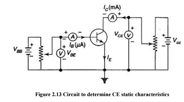
Input Characteristics
It is defined as the characteristic curve drawn between input voltages to input current whereas output voltage is constant.
To determine input characteristics, the collector base voltage VCB is kept constant at zero and base current IB is increased from zero by increasing VBE.This is repeated for higher fixed values of VCE.
A curve is drawn between base current and base emitter voltage at constant collector base voltage is shown in figure2.14. Here the base width decreases. So curve moves right as VCE increases.
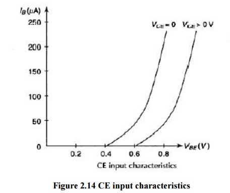
Figure 2.14 CE input characteristics
Output Characteristics
It is defined as the characteristic curve drawn between output voltage to output current whereas input current is constant.
To determine output characteristics, the base current IB is kept constant at zero and collector current Ic is increased from zero by increasing VCE.This is repeated for higher fixed values of IB.
From the characteristic it is seen that for a constant value of IB, Ic is independent of VCB and the curves are parallel to the axis of VCE.
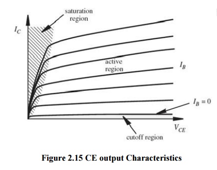
Figure 2.15 CE output Characteristics
The output characteristic has 3 basic regions:
- Active region –defined by the biasing arrangements.
- Cutoff region – region where the collector current is 0A
Saturation region- region of the characteristics to the left of VCB = 0V.
Transistor parameters in CE configuration
The slope of CE characteristics will give the following four transistor parameters. It is known as emitter hybrid parameters.
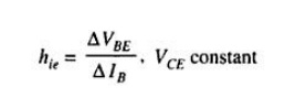
I. Input impedance (hie): It is defined as the ratio of change in input voltage (base voltage) to change in input current (base current) with the output voltage (collector voltage) is kept constant.
II. Output admittance (hoe): It is defined as the ratio of change in output current (collector current) to change in output voltage (collector voltage) with the input current (base current) is kept constant.
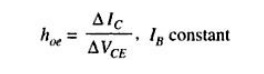
This ranges from 0.1 to 10µ mhos.
III. Forward current gain (hfe): It is defined as the ratio of change in output current (collector current) to change in input current (base current) with the output voltage (collector voltage) is kept constant.
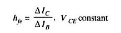
This ranges from 20 to 200.
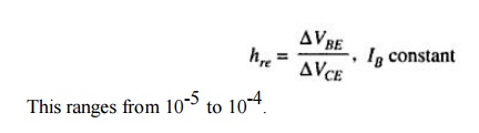
IV. Reverse voltage gain (hre): It is defined as the ratio of change in input voltage (base voltage) to change in output voltage (collector voltage) with the input current (base current) is kept constant.
3 CC CONFIGURATION
In common collector configuration circuit is shown in figure. Here collector is grounded and it is used as the common terminal for both input and output. It is also called as grounded collector configuration. Base is used as a input terminal whereas emitter is the output terminal.
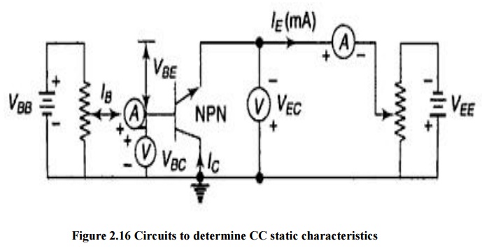
Figure 2.16 Circuits to determine CC static characteristics
Input Characteristics
It is defined as the characteristic curve drawn between input voltage to input current whereas output voltage is constant.
To determine input characteristics, the emitter base voltage VEB is kept constant at zero and base current IB is increased from zero by increasing VBC.This is repeated for higher fixed values of VCE.A curve is drawn between base current and base emitter voltage at constant collector base voltage is shown in figure2.17.
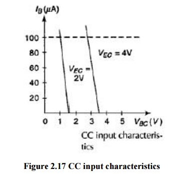
Figure 2.17 CC input characteristics
Output Characteristics
It is defined as the characteristic curve drawn between output voltage to output current whereas input current is constant.
To determine output characteristics, the base current IB is kept constant at zero and emitter current IE is increased from zero by increasing VEC. This is repeated for higher fixed values of IB.
From the characteristic it is seen that for a constant value of IB, IE is independent of VEB and the curves are parallel to the axis of VEC.
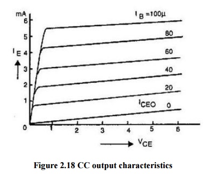
Figure 2.18 CC output characteristics
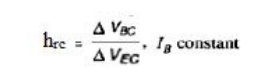
Transistor parameters in CC configuration
The slope of CC characteristics will give the following four transistor parameters. It is known as base hybrid parameters.
I. Input impedance (hic): It is defined as the ratio of change in input voltage (base voltage) to change in input current (base current) with the output voltage (emitter voltage) is kept constant.

II. Output admittance (hoc): It is defined as the ratio of change in output current (emitter current) to change in output voltage (emitter voltage) with the input current (base current) is kept constant.

III. Forward current gain (hfc): It is defined as the ratio of change in output current (emitter current) to change in input current (base current) with the output voltage (emitter voltage) is kept constant.

IV. Reverse voltage gain (hrc): It is defined as the ratio of change in input voltage (base voltage) to change in output voltage (emitter voltage) with the input current (base current) is kept constant.
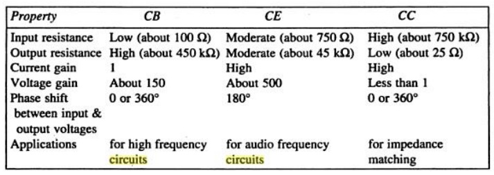
A comparison of CB, CE and CC Configurations
6 Hybrid-Pi Model
The hybrid-pi model is a po pular circuit model used for analyzing the small signal behavior of bipolar junction and field effect transistors. Sometimes it is also called Giacoletto model. The model can be quite accurate for low-frequency circuits and can easil y be adapted for higher frequency circuits with the ad dition of appropriate inter-electrode capacitances and other parasitic elements.
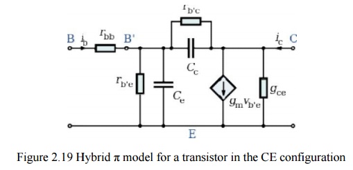
Figure 2.19 H ybrid π model for a transistor in the CE configuration
Where,
rbb- base spreading resistance between the actual base B and virtual base B’. It represents the bulk resistance of the base. Its typi cal value is 100Ω.
- resistance between the virtual base B’ and the emitter terminal E whose typical value is 1kΩ.
- Resistance between the virtual base B’and the collector terminal C w hose typical value is
4MΩ.
- Diffusion capacitance of the normally forward biased base- emitter ju nction. It has a typical value of 100pF.
- Transistor capacitance of the normally reverse biased collector- base junction. It has a typical value of 3pF.
- output resistance with typical value of 80kΩ
- output current genera tor value where gm is the transconductance of the transistor.
Hybrid-π conductance ’s
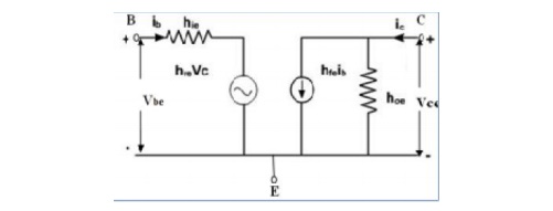
Figure 2.20 h-paramete r model for a common-emitter transistor at low frequency
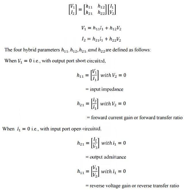
7 h-PARAMETER BJT MODEL
A transistor can be treated as a two port network. The terminal behavior of any two port network can be specified by the terminal voltage Vi and Vo at port 1 and port 2 respectively and currents Ii and Io, entering ports 1 and 2 respectively. As shown in figure 2.20
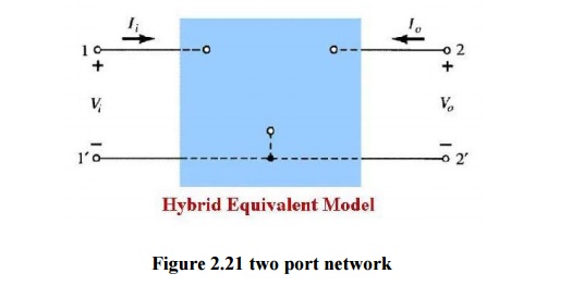
Figure 2.21 two port network
Of these four variables, Vi , Vo ,Ii and Io two can be selected as independent variables and the remaining two can be expressed in terms of these independent variables. This leads to various two port parameters out of which the following are very important.
i. h-parameters or hybrid parameters
ii. Z-parameters or impedance parameters
iii. Y-parameters or admittance parameters
The h-parameter model is typically suited to transistor circuit modeling. Hence, both short-circuit and open-circuit terminal conditions are used. It is important because:
1. Its values are used on specification sheets
2. It is one model that may be used to analyze circuit behavior
3. It may be used to form the basis of a more accurate transistor model
The h parameter model has values that are complex numbers that vary as a function of:
1. Frequency
2. Ambient temperature
3. Q-Point
At low and mid- band frequencies, the h parameter values are real values. Other models exist because this model is not suited for circuit analysis at high frequencies.
If the input current and the output voltage are taken as independent variables, the input voltage and output current can be written as
The equivalent circuit of the h-parameter representation is shown in figure 2.. Here h12V2 is the controlled voltage source and h21I2 is the controlled current source.
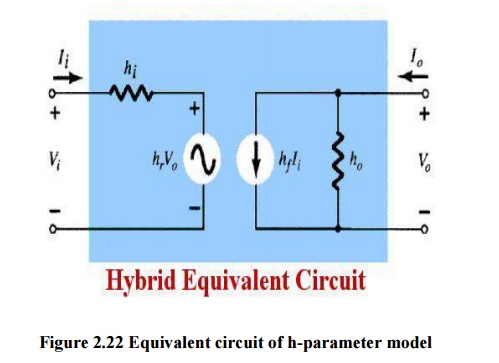
Figure 2.22 Equivalent circuit of h-parameter model
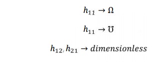
The alternative subscript notations recommended by IEEE commonly used are
i=11=input, o=22=output
f=21=forward transfer, r=12=reverse transfer
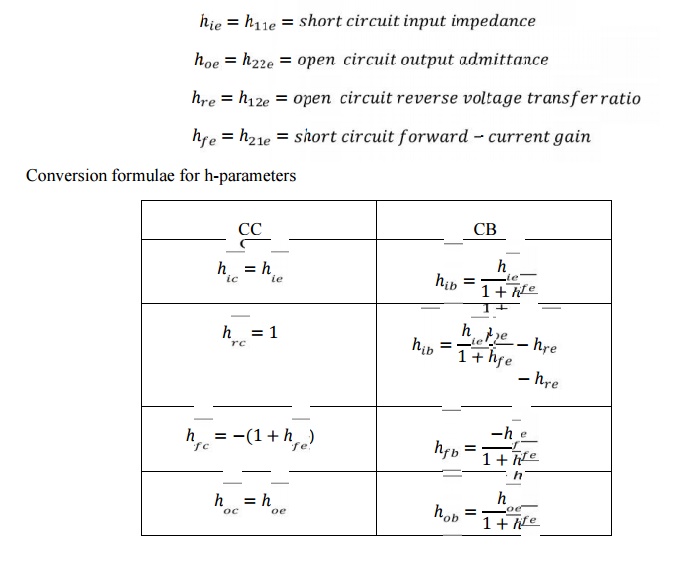
When h-parameters are applied to transistors, it is a common practice to add a second subscript to designate the type of configuration. Considered –e for common emitter, b for common base and and c for common collector. Thus, for a common emitter (CE) configuration,
8 Ebers-Moll Model
The Ebers-Moll model, or equivalent circuit, is one of the classic models of the bipolar transistor. This particular model is based on the interacting diode junctions and applicable in any of the transistor operating modes.
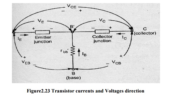
Figure2.23 Transistor currents and Voltages direction
The general expression for collector current IC of a transistor for any voltage across collector junction VC and emitter current IE is
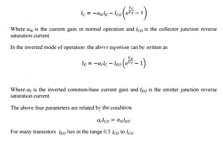
Figure 2.24 Ebers-moll models for a PNP transistor
In above figure, two separate ideal diodes are connected back to back with saturation currents-and - and there are two dependent current-controlled sources shunting the ideal diodes. The current
sources account for the minority carrier transport across the base. An application of kirchhoff’s current law to the collector node of the above figure gives
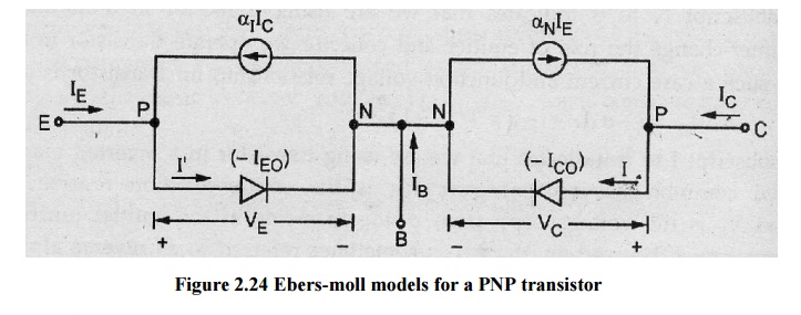
Which is nothing but the general expression for collector current of a transistor. Hence this model is valid for both forward and reverse static voltages applied across the transistor junctions.
9 Gummel-Poon Model
The DC and dynamic currents of the transistor in response to VBE and VCE can be represented accurately by BJT model used in circuit simulators such as Spice. The Gummel-Poon model of the BJT considers more physics of the transistor that the Ebers-Moll model. This model can be used if, for example, there is a non-uniform doping concentration in the base.
The Gummel–Poon model is a detailed charge-controlled model of BJT dynamics, which has been adopted and elaborated by others to explain transistor dynamics in greater detail than the terminal-based models typically do.This model also includes the dependence of transistor β-values upon the dc current levels in the transistor, which are assumed current-independent in the Ebers–Moll model.
A significant effect included in the Gummel–Poon model is the DC current variation of the transistor βF and βR.
– When certain parameters are omitted, the Gummel–Poon model reverts to the simpler Ebers–Moll model.
The Gummel–Poon model and modern variants of it are widely used via incorporation in the SPICE.The Gummel-Poon model is valid for both positive and negative values of VBE and VCE where as the ebers-moll model is limited to positive values of VBE and VCE. Gummel –poon was an improvement over the ebers-moll model by taking into account the early effect and high level injection effects.
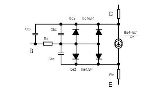
Figure 2.25 Gummel-Poon model with high-level injection effect and early effect
10Multi Emitter Transistors (Transistor Transistor Logic)
A Multiple-emitter transistor is a specialized bipolar transistor mostly used at the inputs of TTL NAND logic gates. Input signals are applied to the emitters. Collector current stops flowing only if all emitters are driven by the logical high voltage, thus performing an AND logical operation using a single transistor. Multiple-emitter transistors replace diodes of DTL and allow reduction of switching time and power dissipation.
TTL inputs are the emitters of a multiple-emitter transistor. This IC structure is functionally equivalent to multiple transistors where the bases and collectors are tied together. The output is buffered by a common emitter amplifier.
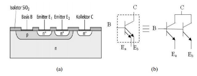
Figure 2.26 Multi-emitter transistor (a) cross-sectional view, (b) symbol
Inputs both logical ones. When all the inputs are held at high voltage, the base– emitter junctions of the multiple-emitter transistor are reverse-biased. Unlike DTL, a small ―collector‖ current (approximately 10µ A) is drawn by each of the inputs. This is because the transistor is in reverse-active mode. An approximately constant current flows from the positive rail, through the resistor and into the base of the multiple emitter transistor. This current passes through the base- emitter junction of the output transistor, allowing it to conduct and pulling the output voltage low (logical zero).
An input logical zero. Note that the base-collector junction of the multiple-emitter transistor and the base-emitter junction of the output transistor are in series between the bottom of the resistor and ground. If one input voltage becomes zero, the corresponding base-emitter junction of the multiple-emitter transistor is in parallel with these two junctions.
A phenomenon called current steering means that when two voltage-stable elements with different threshold voltages are connected in parallel, the current flows through the path with the smaller threshold voltage. As a result, no current flows through the base of the output transistor, causing it to stop conducting and the output voltage becomes high (logical one). During the transition the input transistor is briefly in its active region; so it draws a large current away from the base of the output transistor and thus quickly discharges its base. This is a critical advantage of TTL over DTL that speeds up the transition over a diode input structure.
The main disadvantage of TTL with a simple output stage is the relatively high output resistance at output logical "1" that is completely determined by the output collector resistor. It limits the number of inputs that can be connected (the fanout). Some advantage of the simple output stage is the high voltage level (up to VCC) of the output logical "1" when the output is not loaded.
Features of Multi-Emitter Structure
· Each emitter strip can be considered as the emitter of a separate transistor and each of these devices share a common base and collector.
· The lateral and vertical dimensions of the emitter can be scaled more easily.
· Aluminium contact spiking in the emitter base junction is minimized.
· The current gain is 3 to 7 times that of a conventional transistor.
· Higher cut off frequency - 17 to 30 Ghz
· Less delay - 50psec gate delay
· Component density of IC is enhanced by the efficient utilization of the chip area.
· It is used particularly in the first stages of the TTL family gates.
· Multi emitter transistor have been fabricated with more than 60 emitter strips.
· Multiple-emitter transistors allows reduction of switching time and power dissipation.
Related Topics