Chapter: Electronic Devices : Bipolar Junction
Important short Questions and Answers: Bipolar Junction
BIPOLAR JUNCTION
1. What
is a transistor? What are the types?
Transistor
consists of two junctions formed by sandwiching either p type or n type
semiconductor between a pair of opposite types.
Two types
- *NPN transistor *PNP transistor
2. Define
BJT?
A bipolar
junction transistor is a three terminal semiconductor device in which the
operation depends on the interaction of both majority and minority carriers and
hence the name bipolar.
3. Give
the hie and heo equations of BJT?
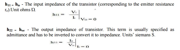
h11 = hie - The
input impedance of the transistor (corresponding to the emitter resistance
re).Unit ohms Ώ.
h22=hoe - The output
impedance of transistor.
This term is
usually specified as admittance and has to be inverted to
convert it to impedance. Units’ siemans S.
4. Why
is the transistor called a current controlled device?
A
transistor is called a current controlled device. This is because; collector
current is controlled by base current. The changes in collector current are
proportional to the corresponding changes in base current.
5. Explain
about the characteristics of a transistor?
In common
emitter configuration, input characteristics is the plot obtained by tracing
the variation of input current IB with the input voltage VBE. Similarly, the
variation of output current IC with the Collector to emitter voltage VCE is
known as output characteristics.
6. Define
h parameters?
One of a
set of four transistor equivalent-circuit parameters that conveniently specify
transistor performance for small voltages and currents in a particular circuit.
Also known as hybrid parameter.
7. Why
we use h-parameters to describe a transistor?
Any
linear circuit can be analyzed by four parameters (input resistance, reverse
voltage gain, forward current gain and output admittance) of mixed dimensions.
Since the dimensions of the parameters have mixed units they are referred as
h-parameters. The h-parameters are determined by both open circuit and short
circuit terminations.
8. What
is operating point?
The Q
point or quiescent point or operating point where DC load line intersects
proper base current curve. The coordinates of Q point decides the zero values
of IC and VCE in a common emitter transistor.
9. In a
bipolar transistor which region is wider and which region is thinner? Why?
The
middle region of bipolar junction transistor is called as the base of the
transistor. Input signal of small amplitude is applied to the base. This region
is thin and lightly doped. The magnified output signal is obtained at the
collector. This region is thick and heavily doped.
10. What
do you understand by thermal runaway?
The
excess heat produced at the collector base junction may even burn and destroy
the transistor. The self destruction of an unbiased transistor is known as
thermal runaway. To avoid thermal run away the operating point of the circuit
is to be stabilized.
11. Define
the delay time and rise time in the switching characteristics of transistor?
In the
transistor switching characteristics the delay time is the time that elapses
the application of the input pulse and current to rise to 10 percent of its
maximum value. The time required for IC to reach 90% of its maximum level from
10% level is called the rise time.
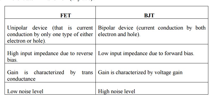
12. Differentiate FET and BJT (any two)?
13. When a
transistor is used as a switch, in which region of output characteristics it is
operated?
When a
transistor is used as a switch it is operated alternately in the cut off region
and saturation region of the output characteristics.
14. When does a transistor act as a switch?
A
transistor should be operated in saturation and cut off regions to use it as a
switch. While operating in saturation region, transistor carry heavy current
hence considered as ON state. In cut-off, it carries no current and it is
equivalent to open switch.
15. Why do the output characteristics of a CB
transistor have a slight upward slope?
The
emitter and collector are forward biased under the saturation region. Hence a
small change in collector voltage causes a significant change in collector
current. Therefore the slight upward slope is found in output characteristics.
16. Define transport factor, β?
It is the
ratio of injected carrier current reaching at collector base junction to
injected carrier current at emitter base junction.
β = I pC
/ I PE

17. Define rise time?
The time
required for IC to reach 90% of its maximum level from 10% level is called rise
time, tr
18. Define current gain in CE configuration?
The
current gain (β) of common emitter configuration is defined as the ratio of
change in collector current to change in base current when collector emitter
voltage is kept constant.
IC / I B
β is also referred as hfe.
19. What is meant by biasing a transistor?
Process
of maintaining proper flow of zero signal collector current and collector
emitter voltage during the passage of signal. Biasing keeps emitter base
junction forward biased and collector base junction reverse biased during the
passage of signal.
20. What
are the various methods used for transistor biasing? Which one is popular?
Base
resistor method
Biasing
with feedback resistor
Voltage
divider bias
Voltage
divider bias is wide popular because it offers excellent stabilization to the
circuit.
21. What
are the limitations of h-parameters?
Obtaining
the exact value of h-parameters for a particular transistor is quite difficult.
Highly suitable only for small ac signals.
22. What
is the basic difference between bias compensation and stabilization?
Stabilization
is the process of making operating point independent of temperature variations
or changes in transistor parameters using dc biasing circuits. In the case of
compensation technique, in order to stabilize the Q point, we use temperature
sensitive devices like diodes, thermistors, transistors instead of DC biasing
circuits.
23. List
the 3 sources of instability of collector current?
• Individual variations
• Temperature dependence of collector
• current Thermal runaway
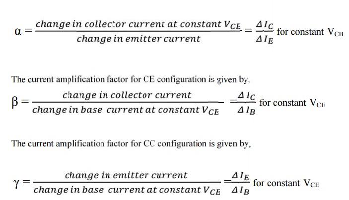
24. Define
Current Amplification Factor for CE, CC, CB Configuration
25. Define
punch through or reach through.
Extremely
large collector voltage, the effective base width may be reduced to zero,
resulting in voltage breakdown of a transistor. This phenomenon is known as
punch through.
26. Define
pinch off voltage
Pinch off
voltage is defined as the drain to source voltage above which drain current
becomes almost constant.
27. A)What
happens to transistor when both the junctions are reverse biased?
B) Can
transistor circuit be operated as a switch? State how?
A) The transistor operated in cut-off region
and act as a open switch.
B) A Transistor can be operated as a closed
or ON Switch, when both the junctions are forward bias and open or OFF switch
when both junction are reverse biased.
Related Topics