Chapter: High Voltage Engineering : High Voltage Testing of Electrical Power Apparatus
Partial Discharge(PD) currents
Partial Discharge(PD) currents
Before
discussing the fundamentals of the measurement of the apparent charge some
remarks concerning the PD currents i will be helpful, as much of the research
work has been and is still devoted to these currents, which are difficult to
measure with high accuracy. The difficulties arise for several reasons. If V is
an a.c. voltage, the main contribution of the currents flowing within the
branches CK and Ct of Fig. 5.10 are displacement currents C dV/dt, and both are
nearly in phase. The PD pulse currents i with crest values in the range of
sometimes smaller than 104 A, are not only small in amplitude, but also of very
short duration. If no stray capacitance in parallel to CK were present, I would
be the same in both branches, but of opposite polarity. For accurate
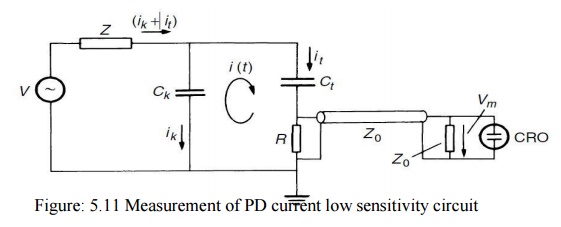
measurements, a shunt resistor with matched coaxial cable may be introduced in
the circuit as shown in Fig. 5.11. The voltage across the CRO(or transient
recorder) input .Only if the capacitance of the test object is small, which is
a special case, will the voltages referring to the PD currents i be clearly
distinguished from the displacement currents i
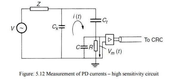
Improvements
are possible by inserting an amplifier (e.g. active voltage probe) of very high
bandwidth at the input end of the signal cable. In this way the signal cable is
electrically disconnected from R. High values of R,however, will introduce
measuring errors, which are explained with Fig. 5.12.A capacitance C of some 10
pF, which accounts for the lead between Ctand earth as well as for the input
capacitance of the amplifier or other stray capacitances, will shunt the
resistance R and thus bypass or delay the very high-frequency components of the
current i. Thus, if i is a very short current pulse, its shape and crest value
are heavily distorted, as C will act as an integrator. Furthermore, with R
within the discharge circuit, the current pulse will be lengthened, as the
charge transfer even with C D 0 will be delayed by a time constant RCtCK/Ct C
CK. Both effects are influencing the shape of the original current pulse, and
thus the measurement of i is a tedious task and is only made for research
purposes.
All
measured data on current shapes published in many papers are suffering from
this effect. One may, however, summarize the results by the following
statements. Partial discharge currents originated in voids within solids or
liquids are very short current pulses of less than a few nanoseconds duration.
This can be understood, as the gas discharge process within a very limited
space is developed in a very short time and is terminated by the limited space
for movement of the charge carriers. Discharges within a homogeneous dielectric
material, i.e. a gas, produce PD currents with a very short rise time5nsec and
a longer tail. Whereas the fast current rise is produced by the fast avalanche
processes the decay of the current can be attributed to the drift velocity of
attached electrons and positive ions within the dielectric. Discharge pulses in
atmospheric air provide in general current pulses of less than about 100 nsec
duration.
Longer
current pulses have only been measured for partial discharges in fluids or
solid materials without pronounced voids, if a number of consecutive discharges
take place within a short time. In most of these cases the total duration of I
is less than about 1 μsec, with only some exceptions e.g. the usual bursts of
discharges in insulating fluids. All these statements refer to test circuits
with very low inductance and proper damping effects within the loop CK Ct. The
current I however, may oscillate, as oscillations are readily excited by the
sudden voltage drop across Ct. Test objects with inherent inductivity or
internal resonant circuits,e.g. transformer or reactor/generator windings, will
always cause oscillatory current pulses. Such distortions of the PD currents,
however, do not change the transferred charge magnitudes, as no discharge
resistor is in parallel to CKor Ct. To quantify the‘ individual apparent charge
magnitudes‘ qi for the repeatedly occurring PDpulses which may have quite
specific statistical distributions, a measuring system must be integrated into
the test circuit which fulfils specific requirements. Already at this point it
shall be mentioned that under practical environment conditions quite different
kinds of disturbances (background noise)are present, which will be summarized
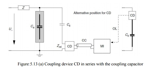
in a later section. Most PD measuring systems applied are integrated into the
test circuit in accordance with schemes shown in Figs 5.13 (a) and (b), which
are taken from the new IEC
Standard31
which replaces the former one as issued in 1981.Within these ‗straight
detection circuits‘, the coupling device ‗CD‘ with its input impedance Zmi
forms the input end of the measuring system. As indicated in Fig. 7.20(a), this
device may also be placed at the high-voltage terminal side, which may be
necessary if the test object has one terminal earthed. Optical links are then
used to connect the CD with an instrument instead ofa connecting cable ‗CC‘.
Some
essential requirements and explanations with reference to these figures as
indicated by the standard are cited here: the coupling capacitor Ck shall be of
low inductance design and should exhibit a sufficiently low level of partial
discharges at the specified test voltage to allow the measurement of the
specified partial discharge magnitude.
A higher
level of partial discharges can be tolerated if the measuring system is capable
of separating the discharges from the test object and the coupling capacitor
and measuring them separately; the high-voltage supply shall have sufficiently
low level of background noise to allow the specified partial discharge
magnitude to be measured at the specified test voltage; high-voltage
connections shall have sufficiently low level of background noise to allow the
specified partial discharge magnitude to be measured at the specified test
voltage; an impedance or a filter may be introduced at high voltage to reduce
background noise from the power supply.
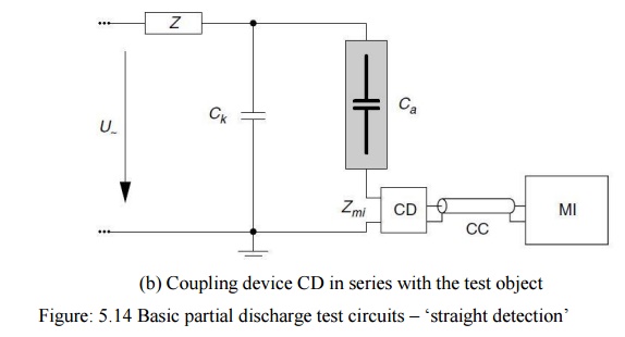
The main
difference between these two types of PD detection circuits is related to the
way the measuring system is inserted into the circuit. InFig.5.13 (a), the CD
is at ground potential and in series to the coupling capacitors as it is
usually done in praxis. In Fig. 5.14(b), CD is in series with the test object Ca.
Here the
stray capacitances of all elements of the high-voltage side to ground potential
will increase the value of Ck providing a somewhat higher sensitivity for this
circuit according to eqn . The disadvantage is the possibility of damage to the
PD measuring system, if the test object fails. The new IEC Standard defines and
quantifies the measuring system characteristics. The most essential ones will
again be cited and further explained below:
The
transfer impedance Zis the ratio of the output voltage amplitude to a constant
input current amplitude, as a function of frequency f, when the input is
sinusoidal. This definition is due to the fact that any kind of output signal
of a measuring instrument (MI) as used for monitoring PD signals is controlled
by a voltage, whereas the input at the CD is a current. The lower and upper
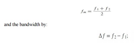
limit frequencies f1 and f2 are the frequencies at which the transfer impedance
Z has fallen by 6 dB from the peak passbandvalue.Midband frequency fm and bandwidth
of: for all kinds of measuring systems, the midland frequency is defined by:
The
superposition error is caused by the overlapping of transient output pulse
responses when the time interval between input current pulses is less than the
duration of a single output response pulse. Superposition errors may be
additive or subtractive depending on the pulse repetition rate n of the input
pulses. In practical circuits both types will occur due to the random nature of
the pulse repetition rate. This rate ‗n‘ is defined as the ratio between the
total number of PD pulses recorded in a selected time interval and the duration
of the time interval.
The pulse
resolution time Tr is the shortest time interval between two consecutive input
pulses of very short duration, of same shape, polarity and charge magnitude for
which the peak value of the resulting response will change by not more than 10
per cent of that for a single pulse. The pulse resolution time is in general
inversely proportional to the bandwidth of the measuring system. It is an
indication of the measuring system‘s ability to resolve successive PD events.
The integration error is the error in apparent charge measurement which occurs
when the upper frequency limit of the PD current pulse amplitudespectrumis
lower than (i) the upper cut-off frequency of a wideband measuring system or
(ii) the mid-band frequency of a narrow-band measuring system. The last
definition of an ‗integration error‘ will need some additional explanation. PD
measuring systems quantifying apparent charge magnitudes are band-pass systems,
which predominantly are able to suppress the high-power frequency displacement
currents including higher harmonics. The lower frequency limit of the band-pass
f1 and the kind of ‗roll-off‘ of the bandpasscontrol this ability. Adequate
integration can thus only be made if the‘ pass-band‘ or the flat part of the
filter is still within the constant part of the amplitude frequency spectrum of
the PD pulse to be measured. Figure 5.14,
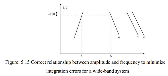
A
band-pass of the measuring system
B
amplitude frequency spectrum of the PD pulse
C
amplitude frequency spectrum of calibration pulse
f1 lower
limit frequency
f2 upper
limit frequency
Again
taken from the new standard, provides at least formal information about correct
relationships. More fundamental information may be found within some specific
literature.
Related Topics