Chapter: Automation, Production Systems, and Computer Integrated Manufacturing : Sensors, Actuators, and Other Control System Components
Digital-to-Analog Conversion and Analog-to-Digital Conversion
ANALOG TO
DIGITAL CONVERSION
Continuous
analog signals from the process must be converted into digital values to be
used by the computer. and digital data
generated by the computer must be converted to analog signals to be used by
analog actuators. We discuss analogladigital conversion in this section and
digitaltoanalog conversion in the following section
Tile
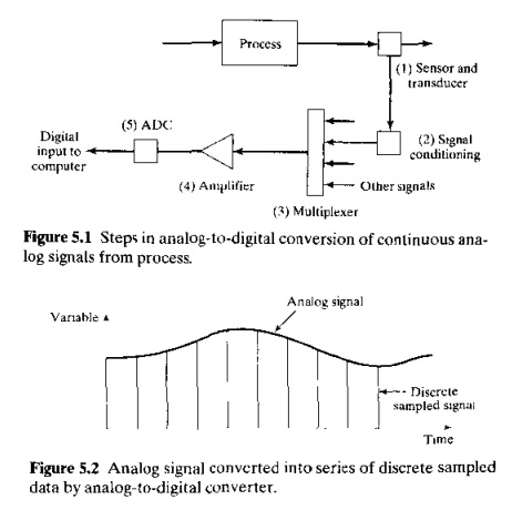
procedure for converting an anaJogsignal from the process into digital fonn
typically consists of the following steps and hardware devices, as illustrated
in Figure 5.1:
Sensor and transducer. This is
the measuring device that generates the analog signal (SectionS.1)
Signal conditioning. The continuous analog
signal from the transducer may require
conditioning
to render it into more suitable form. Common signal conditioning steps include:
(1) filtering to remove random noise and (2) conversion from one signal form to
another, for example, converting a current into a voltage.
Multiplexer. The multiplexer is a switching
device connected in series with each input
channel from the process; it is used to timeshare the analogtodigital
converter (ADC) among the input channels. The alternative is to have a separate
ADC for each input channel. which would he costly for a large application with
many input channels. Since the process variables need only be sampled
periodically, using a multiplexer provides a costeffective alternative to
dedicated ADCs for each channel.
Amplifier. Amplifiers arc used to scale the
incoming signal up or down to be compatible with the range of the
analogtodigital converter.
Analogtndigital converter. As its
name indicates, the function of the ADC is to convert the incoming analog
signal into its digital counterpart.
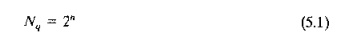
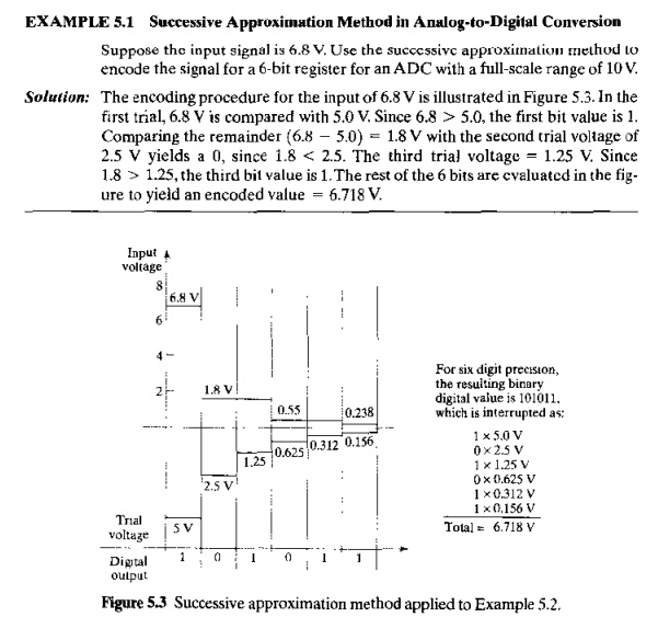
let us consider the operation of the ADC, which is the heart of the conversion process. Analogtodigital conversion occurs in three phases: (1) sampling, (2) quantization, and (3) encoding. Sampling consists of converting the continuous signal into a series of discrete analog signals at periodic intervals. as shown in Figure 5.2. In quantization, each discrete analog signal is assigned to one of a finite number of previously defined amplitude levels. The amplitude levels are discrete values of voltage ranging over the full scale of the ADC In the encoding phase, the discrete amplitude levels obtained during quantization are converted into digital code, representing the amplitude level as a sequence of binary digits.
In
selecting an analog-to-digital converter for a given application, the following
factors are relevant: (I) sampling rate. (2) conversion time, (3) resolution,
and (4) conversion method.
The sampling rate is the rate at which the
continuous analog signals are sampled or polled. Higher sampling rates mean
that the continuous waveform of the analog signal can be more closely
approximated. When the incoming signals are multiplexed, the maximum possible
sampling rate for each signal is the maximum sampling rate of the ADC divided
by the number of channels that arc processed through the multiplexer. For
example, if the maximum sampling rate of the ADC is HX)() sample/sec, and there
are 10 input channels through the multiplexer, then the maximum sampling rate
for each input line is 1000/10 = 100
sample/sec. (This ignores time losses due 10 multiplexer switching.)
The
maximum possible sampling rate of an A DC is limited by the ADC conversion
time. Conversion time of an ADC is
the time interval between when an incoming signal is applied and when the
digital value is determined by the quantization and encoding phases of the
conversion procedure. Conversion time depends on (1) number of bits n used to define the converted digital
value; as n is increased, conversion
time increases (bad news), but resolution of the ADC improves (good news); and (2)
type of conversion procedure used by the ADC
The resolution of an ADC is the precision
with which the analog signal is evaluated. Since the signal is represented in
binary form, precision is determined by the number of quantization levels,
which in turn is determined by the bit capacity of the ADC and the computer.
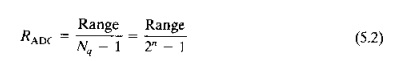
lhe number of quantization levels is defined as follows
where Nq ~ number of quantization levels:
and n = number
of bits. Resolution can be defined in equation form as follows:
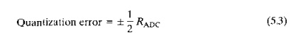
where R(ADC) = resolution of the Anc. also called the quarui
zationlevei spacing, which is the length of each quantization level; Range = fullscale range of the ADC,
usually 010 V (the incoming signal must typically be amplified, either up or
down, to this range); and N., = the number of quantization
levels, defined in Eq. (5.1).
Quantization
generates an error, because the quantized digital value is likely to be
different from the true value of the analog signal. The maximum possible error
occurs when the true value of the analog signal is on the horderline between
two adjacent quantization levels; in
this case. the error is onehalf
the quantizationlevel spacing. By this
reasoning, the quantiration error is
defined:
Various conversion methods arc available by
which to encode an analog signal into its digital equivalent. Let us discuss
one of the most common tcchniqucs,calted the succe.\sive approximation
method. In this method, a series of known trial voltages are successively compared to the input signal whose
value is unknown. The number of trial voltages corresponds to the number of
bits used 10 encode the signal. The first trial voltage is onehalf the
fullscale range of the ADC, and each successive trial voltage is onehalf the
preceding value, Comparing the remainder of the input voltage with each trial
voltage yields a bit value of"I" if the input exceeds the trial value
and "0" if the input is less than the
trial voltage. The successive hit values, multiplied by their corresponding
trial voltage values, provide the encoded value of the input signal. Let us
illustrate the procedure with an example.
DIGITAL-TO-ANALOG
CONVERSION
where Eo = output
voltage of the decoding step (V); Eler = reference voltage (V); and 81.82, ,B,; = status of successive bits in the
register.O or 1.and n = the number of bits in the binary
registcr ,
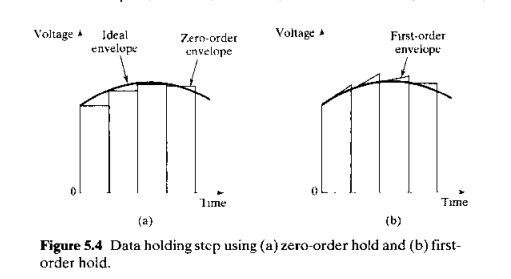
T'he obccuve
in the data holding step ts 10 approximate the envelope termed by the data
series, as illustrated in Figure 5.4. Data holding devices are classified
according to the order of the extrapolation calculation used to determine the
voltage output Juring sampling intervals. The most common extrapolator is a zeroorder hold, in which the output
voltage between sampling instants is a sequence of step signals, as in Figure
5.4([1). The voltage function Juring the sampling interval is constant and can
be expressed very simply as:
where E(r} = voltage as a function of time I
during the sampling interval (V), and Eo
= voltage
output from the decoding step, Eq. (5.4).
The
first-order data hold is less common than the zero-order hold, but it usually
approximates the envelope of the sampled data values more closely. With the first-order hold, the voltage function £(t) during the sampling interval
changes with a constant slope determined by the two preceding E" values. Expressing this
mathematically, we have
where a = rate of change of E(t), Eo
= output voltage from Eq.(5.4) at
the start of the sampling interval (V), and t = time {secl.The value of a
is computed each sampling interval as follows:
where Eo = output
voltage from Eq. (5A) at the stan of
the sampling interval (V), T = time interval between sampling
instants (sec), and F.,,(T) = value of
Evfrom Eq.
(5.4) from the preceding sampling instant (removed backward in time by T, V).
The result of the first-order hold is illustrated in Figure 5.4(bl.
A
digital-to-analog converter uses a reference voltage of 100 V and has 6-bit
precision. In three successive sampling instants, 0.5 sec apart, the data
contained in the binary register are the following'
Determine:
(a) the decoder output values for the three sampling instants and the voltage
signals between instants 2 and 3 for (b) a zeroorder hold and (c) a first-order
hold.
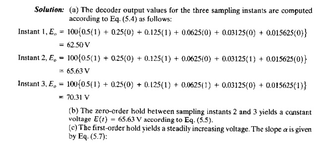
The zero-order hold between sampling instants 2 and
3 yields a constant voltage E(t) = 65.63 V according to Eq. (5.5).
The
first-order hold yields a steadily increasing voltage. The slope a is given by Eq. (5.7):
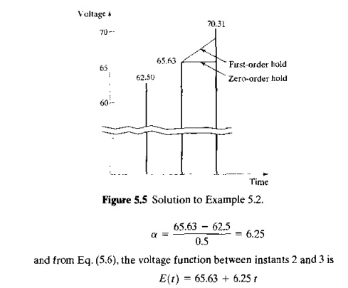
These
values and functions are plotted in Figure 5.5. Note that the firstorder hold
more accurately anticipates the value of EQ at sampling instant 3 than does
the zero-order hold.
Related Topics