Chapter: Electronic Devices and Circuits : Amplifiers
CE, CB and CC Amplifiers Circuits
BJT SMALL SIGNAL MODEL
1. CE, CB and CC Amplifiers:
An amplifier is used to increase the signal level. It is used to get a larger signal output from a small signal input. Assume a sinusoidal signal at the input of the amplifier. At the output, signal must remain sinusoidal in waveform with frequency same as that of input. To make the transistor work as an amplifier, it is to be biased to operate in active region. It means base-emitter junction is forward biased and base-collector junction is reverse biased.
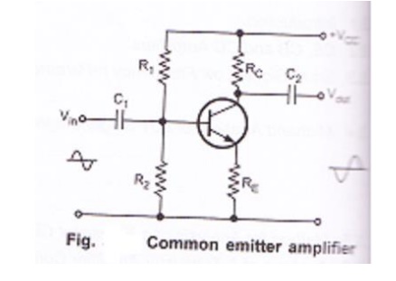
Let us consider the common emitter amplifier circuit using voltage divider bias.
In the absence of input signal, only D.C. voltage is present in the circuit. It is known as zero signal or no signal condition or quiescent condition. D.C. collector-emitter voltage VCE, D.C. collector current IC and base current IB is the quiescent operating point for the amplifier. Due to this base current varies sinusoidaly as shown in the below figure.
Fig. IBQ is quiescent DC base current
If the transistor is biased to operate in active region, output is linearly proportional to the input.
The collector current is β times larger than the input base current in CE configuration. The collector current will also vary sinusoidally about its quiescent value ICQ. The output voltage will also vary sinusoidally as shown in the below figure.
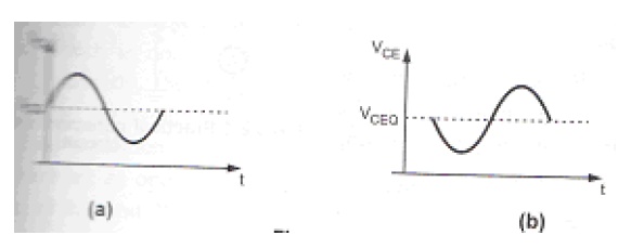
Variations in the collector current and voltage between collector and emitter due to change in base current are shown graphically with the help of load line in the above figure.
2. Common Emitter Amplifier Circuit:
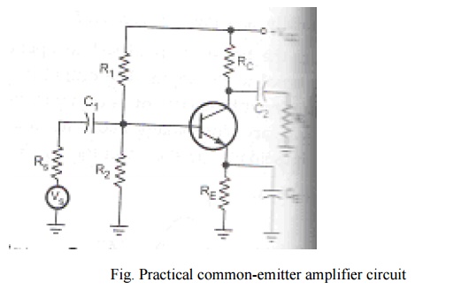
From above circuit, it consists of different circuit components. The functions of these components are as follows:
1. Biasing Circuit:
Resistors R1, R2 and RE forms the voltage divider biasing circuit for CE amplifier and it sets the proper operating point for CE amplifier.
2. Input Capacitor C1:
C1 couples the signal to base of the transistor. It blocks any D.C. component present in the signal and passes only A.C. signal for amplification.
3. Emitter Bypass Capacitor CE:
CE is connected in parallel with emitter resistance RE to provide a low reactance path to the amplified A.C. This will reduce the output voltage and reducing the gain value.
4. Output Coupling Capacitor C2:
C2 couples the output of the amplifier to the load or to the next stage of the amplifier. It blocks D.C. and passes only A.C. part of the amplified signal.
Need for C1, C2, and CE:
The impedance of the capacitor is given by,
XC = 1/ (2∏fc)
Phase reversal:
The phase relationship between the input and output voltages can be determined by considering the effect of positive and negative half cycle separately. The collector current is β times the base current, so the collector current will also increases. This increases the voltage drop across RC.
VC = VCC - ICRC
Increase in IC results in a drop in collector voltage VC, as VCC is constant. Vi increases in a positive direction, Vo goes in negative direction and negative half cycle of output voltage can be obtained for positive half cycle at the input.
In negative half cycle of input, A.C. and D.C. voltage will oppose each other. This will reduce the base current. Accordingly collector current and drop across RC both will reduce and it increases the output voltage. So positive half cycle at the output for negative half cycle at the input can be obtained. So there is a phase shift of 180º between input and output voltages for a common emitter amplifier.
3. Common Collector Amplifier Circuit:
From above circuit, D.C. biasing is provided by R1, R2 and RE. The load resistance is capacitor coupled to the emitter terminal of the transistor. When a signal is applied to base of the transistor, VB is increased and decreased as the signal goes positive and negative respectively.
From figure, VE = VB - VBE
Consider VBE is constant, so the variation in VB appears at emitter and emitter voltage VE will vary same as base voltage VB. In common collector circuit, emitter terminal follows the signal voltage applied to the base. It is also known as emitter follower.
4. Common Base Amplifier Circuit:
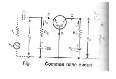
From above circuit, the signal source is coupled to the emitter of the transistor through C1. The load resistance RL is coupled to the collector of the transistor through C2. The positive going pulse of input source increases the emitter voltage. As base voltage is constant, forward bias of emitter-base junction reduces. This reduces Ib, Ic and drop across Rc.
Vo = VCC - ICRC
Reduction in IC results in an increase in Vo. Positive going input produces positive going output and vice versa. So there is no phase shift between input and output in common base amplifier.
Related Topics