Chapter: Electronic Devices and Circuits : Amplifiers
MOSFET small signal model Amplifiers
MOSFET small signal model Amplifiers
It provides an excellent voltage gain with high input impedance. Due to these characteristics, it is often preferred over BJT.
Three basic FET configurations
Common source, common drain and common gate
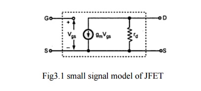
1. MOSFET low frequency a.c Equivalent circuit
Figure shows the small signal low frequency a.c Equivalent circuit for n-channel JFET.
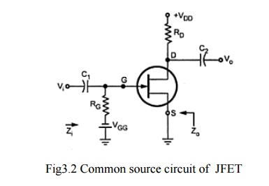
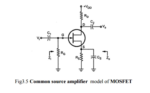
ü Common Source Amplifier With Fixed Bias
Figure shows Common Source Amplifier With Fixed Bias. The coupling capacitor C1 and C2 which are used to isolate the d.c biasing from the applied ac signal act as short circuits for ac analysis.
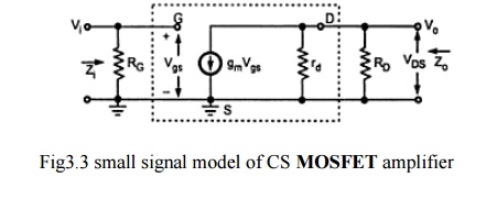
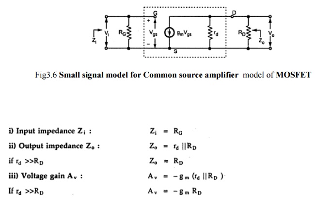
The following figure shows the low frequency equivalent model for Common Source Amplifier With Fixed Bias. It is drawn by replacing
· All capacitors and d.c supply voltages with short circuit
· JFET with its low frequency a.c Equivalent circuit
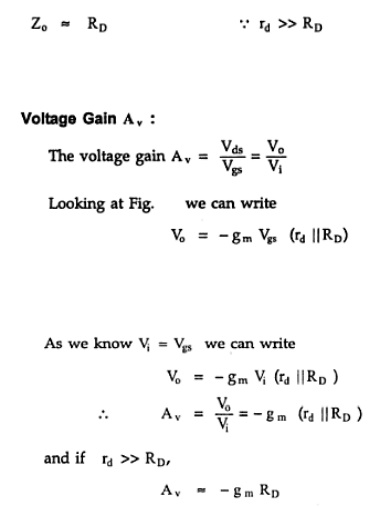
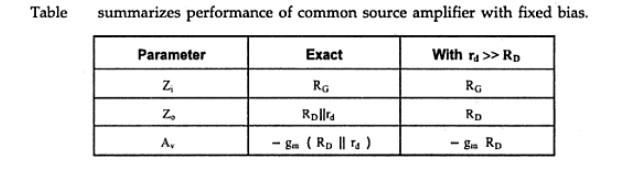
ü Input Impedance Zi
o Zi = RG
ü Output Impedance Zo
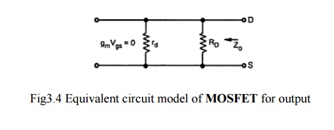
It is the impedance measured looking from the output side with input voltage Vi equal to Zero.
As Vi=0,Vgs =0 and hence gmVgs =0 . And it allows current source to be replaced by an open circuit.

If the resistance rd is sufficiently large compared to RD, then
2. Common source amplifier with self bias(Bypassed Rs)
Figure shows Common Source Amplifier With self Bias. The coupling capacitor C1 and C2 which are used to isolate the d.c biasing from the applied ac signal act as short circuits for ac analysis. Bypass capacitor Cs also acts as a short circuits for low frequency analysis.
The following figure shows the low frequency equivalent model for Common Source Amplifier With self Bias.
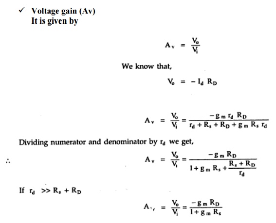
The negative sign in the voltage gain indicates there is a 180o phase shift between input and output voltages.
ü Common source amplifier with self bias (unbypassed Rs)
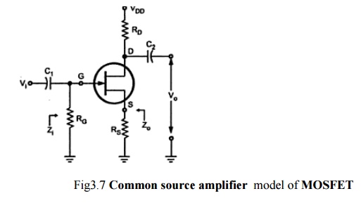
Now Rs will be the part of low frequency equivalent model as shown in figure.
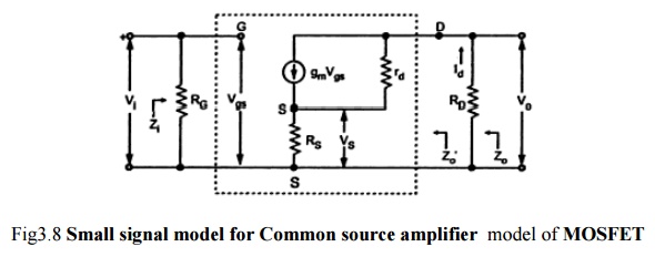
ü Input Impedance Zi
o Zi = RG
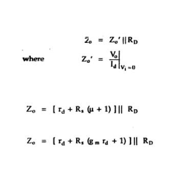
ü Output Impedance Zo
It is given by
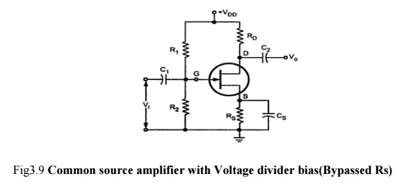
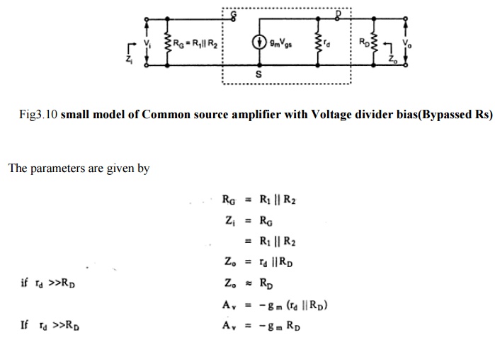
ü Common source amplifier with Voltage divider bias(Bypassed Rs)
Figure shows Common Source Amplifier With voltage divider Bias. The coupling capacitor C1 and C2 which are used to isolate the d.c biasing from the applied ac signal act as short circuits for ac analysis. Bypass capacitor Cs also acts as a short circuits for low frequency analysis.
The following figure shows the low frequency equivalent model for Common Source Amplifier With voltage divider Bias
The negative sign in the voltage gain indicates there is a 180o phase shift between input and output voltages.
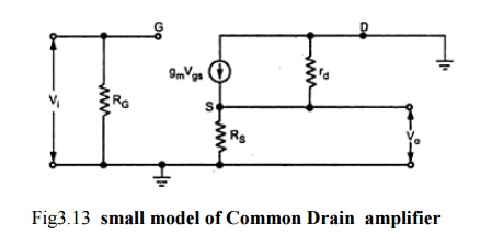
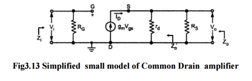
ü Common Drain Amplifier
In this circuit, input is applied between gate and source and output is taken between source and drain.
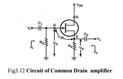
In this circuit, the source voltage is
Vs = VG+VGS
When a signal is applied to the MOSFET gate via C1 ,VG varies with the signal. As VGS is fairly constant and Vs = VG+VGS, Vs varies with Vi.
The following figure shows the low frequency equivalent model for common drain circuit.
Input Impedance Zi
Zi = RG
Output Impedance Zo
It is given by
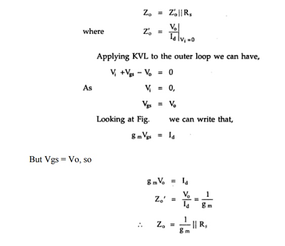
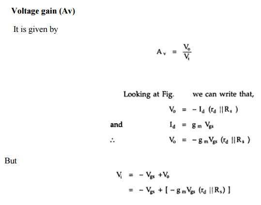
Substitute the value Vo and Vi. Then
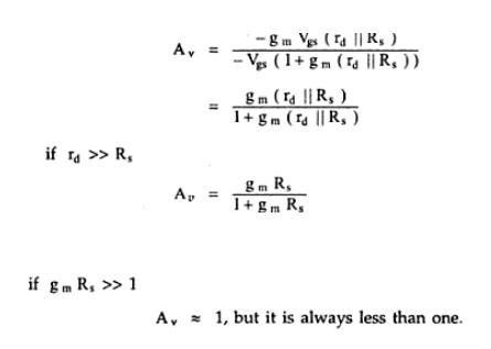
Common drain circuit does not provide voltage gain.& there is no phase shift between input and output voltages.
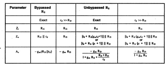
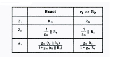
Table summarizes the performance of common drain amplifier
Related Topics