Chapter: Microprocessor and Microcontroller : 8086 Microprocessor
8086 Microprocessor architecture
INTRODUCTION
·
It is a semiconductor device consisting of
electronic logic circuits manufactured by using either a Large scale (LSI) or
Very Large Scale (VLSI) Integration Technique.
·
It includes the ALU, register arrays and control
circuits on a single chip. The microprocessor has a set of instructions,
designed internally, to manipulate data and communicate with peripherals.
·
The era microprocessors in the year 1971, the Intel
introduced the first 4-bit microprocessor is 4004. Using this the first
portable calculator is designed.
·
The 16-bit Microprocessor families are designed
primarily to complete with microcomputers and are oriented towards high-level
languages. They have powerful instruction sets and capable of addressing mega
bytes of memory.
·
The era of 16-bit Microprocessors began in 1974
with the introduction of PACE chip by National Semiconductor. The Texas
Instruments TMS9900 was introduced in the year 1976. The Intel 8086
commercially available in the year 1978, Zilog Z800 in the year 1979, The
Motorola MC68000 in the year 1980.
·
The 16-bit Microprocessors are available in
different pin packages. Ex: Intel 8086/8088 40 pin package Zilog Z8001 40 pin
package, Digital equipment LSI-II 40 pin package, Motorola MC68000 64 pin
package National Semiconductor NS16000 48 pin package.
·
The primary objectives of this 16-bit
Microprocessor can be summarized as follows.
1. Increase
memory addressing capability
2. Increase
execution speed
3. Provide a
powerful instruction set
4. Facilitate
programming in high-level languages.
Microprocessor Architecture:
·
The 8086 CPU is divided into two independent
functional parts, the Bus interface unit (BIU) and execution unit (EU).
The Bus Interface Unit contains
Bus Interface Logic, Segment registers, Memory addressing logic and a Six byte instruction object code queue. The BIU sends
out address, fetches the instructions from memory, read data from ports and
memory, and writes the data to ports and memory.
·
The
execution unit: contains the Data and Address registers, the
Arithmetic and Logic Unit, the
Control Unit and flags. tells the BIU where to fetch instructions or data from,
decodes instructions and executes instruction. The EU contains control
circuitry which directs internal operations. A decoder in the EU translates
instructions fetched from memory into a series of actions which the EU carries
out. The EU is has a 16-bit ALU which can add, subtract, AND, OR, XOR,
increment, decrement, complement or shift binary numbers. The EU is decoding an
instruction or executing an instruction which does not require use of the
buses.
In other
words the BIU handles all transfers of data and addresses on the buses for the
execution unit.
The Queue: The BIU fetches up to 6
instruction bytes for the following instructions. The BIU stores these prefetched bytes in first-in-first-out register set
called a queue. When the EU is ready for its next instruction it simply reads
the instruction byte(s) for the instruction from the queue in the BIU. This is
much faster than sending out an address to the system memory and waiting for
memory to send back the next instruction byte or bytes.
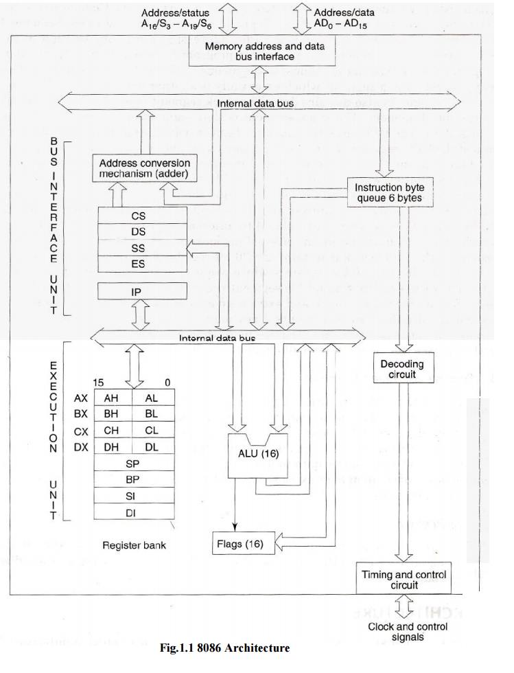
Except in
the case of JMP and CALL instructions, where the queue must be dumped and then
reloaded starting from a new address, this prefetch-and-queue scheme greatly
speeds up processing. Fetching the next instruction while the current
instruction executes is called pipelining.
·
Word
Read: Each of 1 MB memory address of 8086 represents a byte wide location.16-bit
words
will be stored in two consecutive memory locations. If first byte of the data
is stored at an even address, 8086
can read the entire word in one operation.
For example if the 16 bit data is stored at even
address 00520H is 9634H MOV BX, [00520H]
8086
reads the first byte and stores the data in BL and reads the 2nd byte and
stores the data in BH
BL=
(00520H) i.e. BL=34H BH= (00521H) BH=96H
If the
first byte of the data is stored at an odd address, 8086 needs two operations
to read the 16 bit data.
For example if the 16 bit data is stored at even
address 00521H is 3897H MOV BX, [00521H]
In first
operation, 8086 reads the 16 bit data from the 00520H location and stores the
data of 00521H location in register BL and discards the data of 00520H location
In 2nd operation, 8086 reads the 16 bit data from the 00522H
location and stores the data of 00522H location in register BH and discards the
data of 00523H location.
BL=
(00521H) i.e. BL=97H BH= (00522H) BH=38H
·
Byte Read: MOV BH, [Addr]
For Even Address:
Ex: MOV
BH, [00520H]
8086
reads the first byte from 00520 location and stores the data in BH and reads
the 2nd byte from the 00521H location and ignores it
BH =[
00520H]
For Odd Address
MOV BH,
[Addr]
Ex: MOV
BH, [00521H]
8086
reads the first byte from 00520H location and ignores it and reads the 2nd byte
from the 00521 location and stores the data in BH
BH =
[00521H]
·
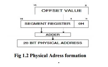
Physical
address formation:
The 8086 addresses a segmented memory. The complete physical address
which is 20-bits long is generated using segment and offset registers each of
the size 16-bit.The content of a segment register also called as segment
address, and content of an offset register also called as offset address. To
get total physical address, put the lower nibble 0H to segment address and add
offset address. The fig 1.3 shows formation of 20-bit physical address.
·
Register
organization of 8086:
All the
registers of 8086 are 16-bit registers. The general purpose registers, can be
used either 8-bit registers or 16-bit registers used for holding the data,
variables and intermediate results temporarily or for other purpose like
counter or for storing offset address for some particular addressing modes etc.
The special purpose registers are used as segment registers, pointers, index
registers or as offset storage registers for particular addressing modes. Fig
1.3
ü AX Register: Accumulator register
consists of two 8-bit registers AL and AH, which can be combined together and used as a 16- bit register AX. AL in
this case contains the low-order byte of the word, and AH contains the
high-order byte. Accumulator can be used for I/O operations, rotate and string
manipulation.
ü BX Register: This register is mainly used as a base register. It holds the starting
base location of a memory region
within a data segment. It is used as offset storage for forming physical
address in case of certain addressing mode.
ü CX Register: It is used as default counter - count register in case of string and
loop instructions.
ü DX Register: Data register can be
used as a port number in I/O operations and
implicit operand or destination in case of few instructions. In integer
32-bit multiply and divide instruction the DX register contains high-order word
of the initial or resulting number.
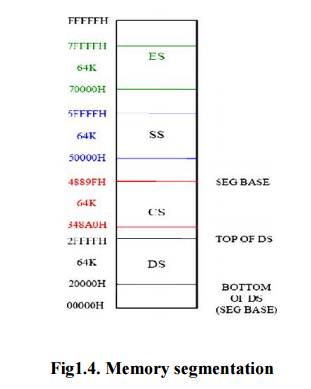
Segment registers:
1Mbyte
memory is divided into 16 logical segments. The complete 1Mbyte memory
segmentation is as shown in fig 1.4. Each segment contains 64Kbyte of memory.
There are four segment registers.
Code segment (CS) is a 16-bit register
containing address of 64 KB segment with
processor instructions. The processor uses CS segment for all accesses to
instructions referenced by instruction pointer (IP) register. CS register
cannot be changed directly.
The CS
register is automatically updated during far jump, far call and far return
instructions. It is used for addressing a memory location in the code segment
of the memory, where the executable program is stored.
ü Stack segment (SS) is a 16-bit register
containing address of 64KB segment with program
stack. By default, the processor assumes that all data referenced by the stack
pointer (SP) and base pointer (BP) registers is located in the stack segment.
SS register can be changed directly using POP instruction. It is used for
addressing stack segment of memory. The stack segment is that segment of
memory, which is used to store stack data.
ü Data segment (DS) is a 16-bit register
containing address of 64KB segment with program
data. By default, the processor assumes that all data referenced by general
registers (AX, BX, CX, DX) and index register (SI, DI) is located in the data
segment. DS register can be changed directly using POP and LDS instructions. It
points to the data segment memory where the data is resided.
ü Extra segment (ES) is a 16-bit register
containing address of 64KB segment, usually
with program data. By default, the processor assumes that the DI register
references the ES segment in string manipulation instructions. ES register can
be changed directly using POP and LES instructions. It also refers to segment
which essentially is another data segment of the memory.
ü It also
contains data.
ü Pointers and index registers.
The
pointers contain within the particular segments. The pointers IP, BP, SP
usually contain offsets within the code, data and stack segments respectively
Stack Pointer (SP) is a
16-bit register pointing to program stack in stack segment.
Base Pointer (BP) is a
16-bit register pointing to data in stack segment. BP register is usually used for based, based indexed
or register indirect addressing.
Source Index (SI) is a
16-bit register. SI is used for indexed, based indexed and register indirect addressing, as well as a
source data addresses in string manipulation instructions.
Destination Index (DI) is a
16-bit register. DI is used for indexed, based indexed and register indirect addressing, as well as a destination data
address in string manipulation instructions.
ü Flag
Register:
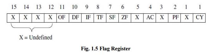
Flags
Register determines the current state of the processor. They are modified
automatically by CPU after mathematical operations, this allows to determine
the type of the result, and to determine conditions to transfer control to
other parts of the program. The 8086 flag register as shown in the fig 1.5.
8086 has 9 active flags and they are divided into two categories:
1. Conditional
Flags
2. Control
Flags
ü Conditional Flags
Carry Flag (CY): This flag indicates an overflow
condition for unsigned integer arithmetic.
It is also used in multiple-precision arithmetic.
Auxiliary Flag (AC): If an
operation performed in ALU generates a carry/barrow from lower nibble (i.e. D0 – D3) to upper nibble (i.e. D4 – D7), the AC
flag is set i.e. carry given by D3 bit to D4 is AC flag. This is not a
general-purpose flag, it is used internally by the Processor to perform Binary
to BCD conversion.
Parity Flag (PF): This flag
is used to indicate the parity of result. If lower order 8-bits of the result contains even number of
1’s, the Parity Flag is set and for odd number of
1’s, the
Parity flag is reset.
Zero Flag (ZF): It is set; if the result of
arithmetic or logical operation is zero else it is reset.
Sign Flag (SF): In sign magnitude format the sign
of number is indicated by MSB bit. If
the result of operation is negative, sign flag is set.
ü Control Flags
Control
flags are set or reset deliberately to control the operations of the execution
unit. Control flags are as follows:
Trap Flag (TF): It is used for single step
control. It allows user to execute one instruction
of a program at a time for debugging. When trap flag is set, program can be run
in single step mode.
Interrupt Flag (IF): It is an
interrupt enable/disable flag. If it is set, the maskable interrupt of 8086 is enabled and if it is reset, the interrupt is
disabled. It can be set by executing instruction sit and can be cleared by
executing CLI instruction.
Direction Flag (DF): It is
used in string operation. If it is set, string bytes are accessed from higher memory address to lower
memory address. When it is reset, the string bytes are accessed from lower
memory address to higher memory address.
Related Topics