Chapter: Linear Integrated Ciruits : Spical ICs
The 555 Timer IC and its Pin Configuration
THE 555 TIMER IC
The 555
is a monolithic timing circuit that can produce accurate & highly stable
time delays or oscillation. The timer basically operates in one of two modes:
either
(i) Monostable
(one - shot) multivibrator or
(ii) Astable
(free running) multivibrator
The
important features of the 555 timer are these:
(i) It
operates on +5v to +18 v supply voltages
(ii) It has an
adjustable duty cycle
(iii) Timing is
from microseconds to hours
(iv) It has a
current o/p
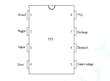
PIN CONFIGURATION OF 555 TIMER:

Pin description: Pin 1: Ground:
All
voltages are measured with respect to this terminal.
Pin 2: Trigger:
The o/p
of the timer depends on the amplitude of the external trigger pulse applied to
this pin.
Pin 3: Output:
There are
2 ways a load can be connected to the o/p terminal either between pin3 &
ground or between pin 3 & supply voltage
i. When
the input is low:
The load
current flows through the load connected between Pin 3 & +Vcc in to the
output terminal & is called the sink current.
(ii) When the output is high:
The
current through the load connected between Pin 3 & +Vcc (i.e. ON load) is
zero. However the output terminal supplies current to the normally OFF load.
This current is called the source current.
Pin 4: Reset:
The 555
timer can be reset (disabled) by applying a negative pulse to this pin. When
the reset function is not in use, the reset terminal should be connected to
+Vcc to avoid any false triggering.
Pin 5: Control voltage:
An
external voltage applied to this terminal changes the threshold as well as
trigger voltage. In other words by connecting a potentiometer between this pin
& GND, the pulse width of the output waveform can be varied. When not used,
the control pin should be bypassed to ground with 0.01 capacitor to prevent any
noise problems.
Pin 6: Threshold:
This is
the non inverting input terminal of upper comparator which monitors the voltage
across the external capacitor.
Pin 7: Discharge:
This pin
is connected internally to the collector of transistor Q1.
When the
output is high Q1 is OFF.
When the
output is low Q is (saturated) ON.
Pin 8: +Vcc: The supply voltage of +5V to +18V
is applied to this pin with respect to ground.
Related Topics