Chapter: Embedded Systems Design : Memory and performance trade-offs
Single cycle processor with large external memory
Scenario 1 — Single cycle
processor with large external memory
In this example, there is a single cycle processor that has to process a
large external table by reading a value, processing it and writing it back.
While the processing level is small — essentially a data fetch, three
processing instructions and a data store — the resulting execution time can be
almost three times longer than expected. The reason is stalling due to data
latency. The first figure shows how the problem can arise.
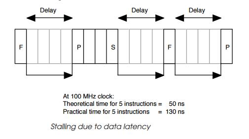
The instruction sequence consists of a data fetch followed by three
instructions that process the information before storing the result. The data
access goes to external memory where there are access delays and therefore the
first processing instruction must wait until the data is available. In this
case, the instruction execution is stalled and thus the fetch instruction takes
the equiva lent of five cycles instead of the expected single cycle. Once the
data has been received, it can be processed and the processing instructions
will continue, one per clock. The final instruction stores the end result and
again this is where further delays can be experienced. The store instruction
experiences the same external memory delays as the fetch instruction. However,
its data is not required by the next set of instructions and therefore the rest
of the instruction stream should be able to continue. This is not the case. The
next instruction is a fetch and has to compete with the external bus interface
which is still in use by the preceding store. As a result, it must also wait
until the transaction is completed.
The next processing instruction now cannot start until the second fetch
instruction is completed. These delays mean that the total time taken at 100
MHz for the five instructions (1 fetch + 3 processing + 1 store) is not 50 ns
but 130 ns — an increase of 2.6 times.
The solution to this involves reordering the code so that the delays are
minimised by overlapping operations. This assumes that the processor can do
this, i.e. the instructions are stored in a separate memory space that can be
accessed simultaneously with data. If not, then this conflict can create
further delays and proces-sor stalls. The basic technique involves moving the
processing segment of the code away from the data access so that the delays do
not cause processing stalls because the data dependencies have been removed. In
other words, the data is already available before the processing instructions
need it.
Moving dependencies can be achieved by restructuring the code so that
the data fetch preceding the processing fetches the data for the next
processing sequence and not the one that imme-diately follows it.
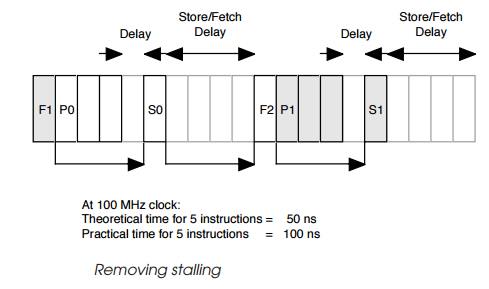
The diagram above shows the general approach. The fetch instruction is
followed by the processing and storage instruction for the preceding fetch.
This involves using an extra register or other local storage to hold the sample
until it is needed but it removes the data dependency. The processing
instructions P0 onward that follow the fetch instruction F1 do not have any
data dependency and thus can carry on processing. The storage in-struction S0
has to wait one cycle until F0 has completed and similarly the fetch
instruction F2 must wait until S0 has finished. These delays are still there
because of the common resource that the store and fetch instructions use, i.e.
the external memory interface. By reordering in this way, the five instruction
sequence is completed twice in every 20 clocks giving a 100 ns timing which is
a significant improvement.
This example also shows that the task in this case is I/O bound in that
the main delays are caused by waiting for data to be fetched or stored. The
processing load could almost be doubled and further interleaved with the store
operations without chang-ing or delaying the data throughput of the system.
What would happen, however, is an increase in the processing load that the
system could handle.
The delays that have been seen are frequently exploited by optimising
routines within many modern compilers. These com-pilers know from information
about the target processor when these types of delays can occur and how to
reschedule instructions to make use of them and regain some of the lost
performance.
Related Topics