Chapter: Electronic Circuits : JFET and MOSFET Amplifiers
Important Short Questions and Answers: JFET and MOSFET Amplifiers
JFET AND MOSFET AMPLIFIERS
1. State the reason for fall in gain at low
frequencies.
The
coupling capacitance has very high reactance at low frequency. Therefore it
will allow only a small part of signal from one stage to next stage and in
addition to that the bypass capacitor cannot bypass or shunt the emitter
resistor effectively. As a result of these factors, the voltage gain rolls of
at low frequency.
2. State the reason for fall in gain at higher
frequencies?
At high
frequency the reactance of coupling capacitor is very low. Therefore it behaves
like a short circuit. As a result of this the loading effect of the next stage
increase which reduces the voltage gain. Hence the voltage gain rolls off at
high frequencies.
3. Why the electrolytic capacitor is not used for
coupling?
Electrolytic
capacitor is a polarized capacitor. So it cannot be used for coupling and also
in electrolytic capacitor, the dielectric is not an insulating material but it
conducting material which will change the capacitance effect.
4. Write a note on effects of coupling capacitor.
The
coupling capacitor Co transmits AC Signal. But blocks Dc. This prevents DC
interferences between various stages and the shifting of operating point.
It
prevents the loading effect between adjacent stages.
5. What is the significance of gain bandwidth
product?
It is
very helpful in the preliminary design of a multistage wideband amplifier. This
can be used to setup a tentative circuit, which is often used for this purpose.
6. Why N-channel FET’s have a better response than
P-channel FET’s?
N-
channel FET have a better high frequency response than P-channel FET due to the
following reason. Mobility of electrons is large in N-channel FET whereas the
mobility of holes is poor in P-channel FET. The input noise is less in N-channel
FET that that of the P-channel FET. The trains conductance is larger in
N-channel FET that that of P-channel Fet.
7. Define Miller effect in input capacitance?
For any
inverting amplifier, the input capacitance will be increased by a miller effect
capacitance, sensitive to the gain of the amplifier and the inter electrode
capacitance connected between the input and output terminals of the active
device.
CMi =
(1-Av) Cf ;
CMo = Cf
Cf =
Inter electrode capacitance between input and output.
8. What is a Darlington connection in the
amplifiers?
A
Darlington transistor connection provides a transistor having a very large
current gain, typically a few thousand. The main features of the Darlington
connection is that the composite transistor acts as a single unit with a
current gain, that is the product of current gains of the individual
transistors.
9. Give the Applications of JFET
FET is
used as a
(1)
Buffer amplifier
(2) Low
Noise Amplifier
(3)
Cascaded Amplifier
(4)
Analog Switch
(5)
Chopper
(6) Phase
Shift Oscillator circuits
(7)
Voltage Variable Resistors in Operational Amplifiers and tone controls etc.,
(8) For
Mixer operation on FM and TV receivers
10. Give the Applications of MOSFET
MOSFETs
can also be used for most applications where JFET is used. MOSFETs have become
very popular for digital logic circuits due to high density of fabrication and
low power dissipation.
(1) MOSFET is
used in Sample and Hold circuit as a switch.
(2) P-MOSFET
and N-MOSFET are used in digital logic circuits
(3) C-MOSFET
is very popular in fabricating of MSI and LSI technology.
11.
Draw a
single stage amplifier circuit using JFET
The
circuit of a Single Stage Common Source N-channel JFET amplifier using self
bias is shown in fig
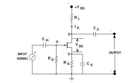
12. What is the purpose of input capacitor, Cin in
single stage common source JFET amplifier?
An ac
signal is supplied to the gate of the FET through an electrolytic capacitor
called input capacitor Cin. This capacitor allows only ac signal enter the gate
but isolates the signal source from RG. If this capacitor is not used, the
signal source resistance will come across the resistor RG and thus changing the
biasing conditions.
13. What is the purpose of Biasing Network (Rs and Cs)
in single stage common source JFET amplifier?
The JFET
is self-biased by using the biasing network Rs- Cs. The desired bias voltage is
obtained when dc component of drain current flows through the source-biasing
resistor Rs. whereas, the capacitor Cs bypasses the ac component of drain
current.
14.
What is
the purpose of Coupling Capacitor (Cc) in single stage common source JFET
amplifier?
It is an
electrolytic capacitor used to couple one stage of amplification to the next
stage or load. It allows only amplified ac signal to pass to the other side but
blocks the dc voltage. If this capacitor is not used, the biasing conditions of
the next stage will be drastically changed due to the shunting effect of Rd.
15.
Give the
expression for ID for E-MOSFET.
ID = (K(VGS - VT)2
16.
What are
the different biasing circuits of FET?
• Fixed
bias circuits
• Self bias
circuits
• Voltage
bias circuits
Related Topics