Chapter: Electronic Circuits : JFET and MOSFET Amplifiers
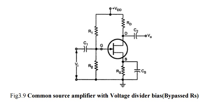
Common source amplifier with Voltage divider bias (Bypassed Rs)
Common source amplifier with
Voltage divider bias (Bypassed Rs)
Figure
shows Common Source Amplifier With voltage divider Bias. The coupling capacitor
C1 and C2 which are used to isolate the d.c biasing from
the applied ac signal act as short circuits for ac analysis. Bypass capacitor
Cs also acts as a short circuits for low frequency analysis.

The
following figure shows the low frequency equivalent model for Common Source
Amplifier With voltage divider Bias

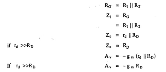
The
parameters are given by

The
negative sign in the voltage gain indicates there is a 180o phase shift
between input and output voltages.
Related Topics