Chapter: Microprocessor and Microcontroller : 8051 Microcontroller
I/O Pins Ports and Circuits of 8051 Microcontroller
I/O ports and circuits
Each port
of 8051 has bidirectional capability. Port 0 is called 'true bidirectional
port' as it floats (tristated) when configured as input. Port-1, 2, 3 are
called 'quasi bidirectional port'. Port-0 Pin Structure Port -0 has 8 pins
(P0.0-P0.7).
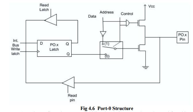
Port-0
can be configured as a normal bidirectional I/O port or it can be used for
address/data interfacing for accessing external memory. When control is '1',
the port is used for address/data interfacing. When the control is '0', the
port can be used as a normal bidirectional I/O port.
Let us assume that control is '0'. When the port is
used as an input port, '1' is written to the latch. In this situation both the
output MOSFETs are 'off'. Hence the output pin floats. This high impedance pin
can be pulled up or low by an external source. When the port is used as an
output port, a '1' written to the latch again turns 'off' both the output
MOSFETs and causes the output pin to float. An external pull-up is required to
output a '1'. But when '0' is written to the latch, the pin is pulled down by
the lower MOSFET. Hence the output becomes zero.
When the
control is '1', address/data bus controls the output driver MOSFETs. If the
address/data bus (internal) is '0', the upper MOSFET is 'off' and the lower
MOSFET is 'on'. The output becomes '0'. If the address/data bus is '1', the
upper transistor is 'on' and the lower transistor is 'off'. Hence the output is
'1'. Hence for normal address/data interfacing (for external memory access) no
pull-up resistors are required.
Port-0
latch is written to with 1's when used for external memory access.
Port-1
Pin Structure Port-1 has 8 pins (P1.1-P1.7) .The structure of a port-1 pin is
shown in fig below.
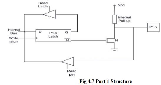
Port-1 does not have any alternate function i.e. it
is dedicated solely for I/O interfacing. When used as output port, the pin is
pulled up or down through internal pull-up. To use port-1 as input port, '1'
has to be written to the latch. In this input mode when '1' is written to the pin
by the external device then it read fine. But when '0' is written to the pin by
the external device then the external source must sink current due to internal
pull-up. If the external device is not able to sink the current the pin voltage
may rise, leading to a possible wrong reading.
PORT 2
Pin Structure Port-2 has 8-pins (P2.0-P2.7) . The structure of a port-2 pin is
shown in figure below:
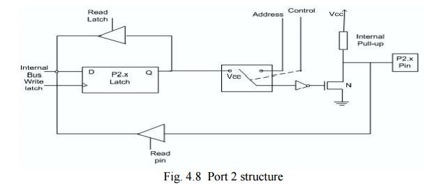
Port-2 is
used for higher external address byte or a normal input/output port. The I/O
operation is similar to Port-1. Port-2 latch remains stable when Port-2 pin are
used for external memory access. Here again due to internal pull-up there is
limited current driving capability.
ü PORT 3 Pin Structure
Port-3
has 8 pin (P3.0-P3.7). Port-3 pins have alternate functions. The structure of a
port-3 pin is shown in figure
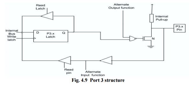
Each pin
of Port-3 can be individually programmed for I/O operation or for alternate
function. The alternate function can be activated only if the corresponding latch
has been written to '1'. To use the port as input port, '1' should be written
to the latch. This port also has internal pull-up and limited current driving
capability.
Interfacing External Memory
If
external program/data memory are to be interfaced, they are interfaced in the
following way.
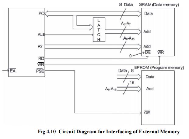
External
program memory is fetched if either of the following two conditions are
satisfied.
1. (Enable
Address) is low. The microcontroller by default starts searching for program
from external program memory.
2. PC is
higher than FFFH for 8051 or 1FFFH for 8052.
PSEN
tells the outside world whether the external memory fetched is program memory
or data memory.
Related Topics