Chapter: Microprocessor and Microcontroller : 8051 Microcontroller
Architecture of 8051
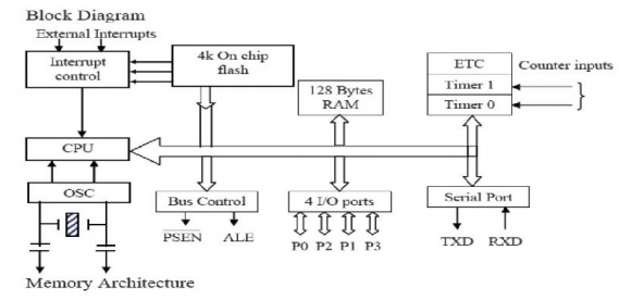
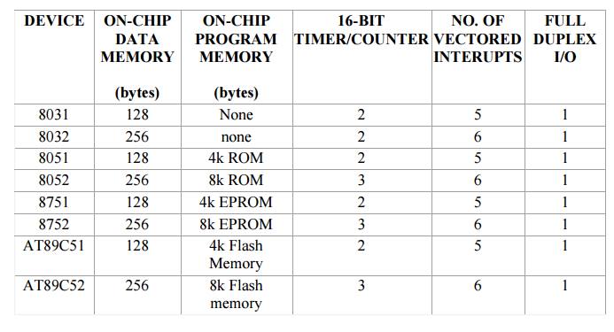
Architecture of 8051:
• It is a
single chip
• Consists
of CPU, Memory
• I/O
ports, timers and other peripherals
• It is a
CPU
• Memory,
I/O Ports to be connected externally.
·
Small size, low power, low cost;
·
Harvard architecture with separate program and data
memory;
·
No data corruption or loss of data; but with
complex circuit
·
The 8051 has three very general types of memory.
·
On-Chip Memory refers to any memory (Code, RAM, or
other) that physically exists on the microcontroller itself. On-chip memory can
be of several types.
·
External Code Memory is code (or program) memory
that resides off-chip. This is often in the form of an external EPROM.
·
External RAM is RAM memory that resides off-chip.
This is often in the form of standard
static RAM or flash RAM.
The 8051
is a flexible microcontroller with a relatively large number of modes of
operations.
Your
program may inspect and/or change the operating mode of the 8051 by
manipulating the values of the 8051's Special Function Registers(SFRs).
SFRs are
accessed as if they were normal Internal RAM. The only difference is that
Internal RAM is from address 00h through 7Fh whereas SFR registers exist in the
address range of 80h through FFh
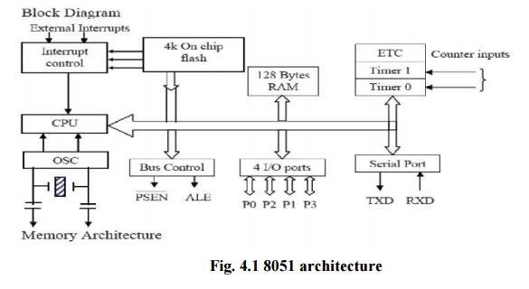
8051 Clock and Instruction Cycle
In 8051,
one instruction cycle consists of twelve (12) clock cycles. Instruction cycle
is sometimes called as Machine cycle by some authors.

In 8051,
each instruction cycle has six states (S 1- S 6). Each
state has two pulses (P1 and P2)
128 bytes of Internal RAM Structure (lower address
space)
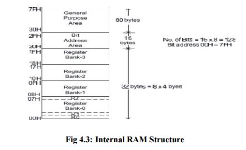
The lower
32 bytes are divided into 4 separate banks. Each register bank has 8 registers
of one byte each. A register bank is selected depending upon two bank select
bits in the PSW register. Next 16bytes are bit addressable. In total, 128bits
(16X8) are available in addressable area. Each bit can be accessed and modified
by suitable instructions. The bit addresses are from 00H (LSB of the first byte
in 20H) to 7FH (MSB of the last byte in 2FH). Remaining 80bytes of RAM are
available for general purpose.
Internal Data Memory and Special Function Register
(SFR) Map
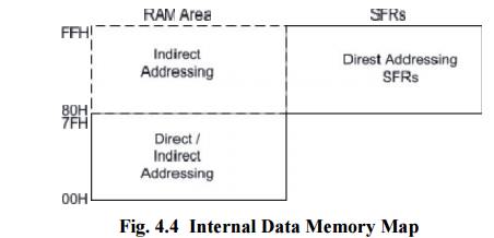
The special function registers (SFRs) are mapped in
the upper 128 bytes of internal data memory address. Hence there is an address
overlap between the upper 128 bytes of data RAM and SFRs. Please note that the
upper 128 bytes of data RAM are present only in the 8052 family. The lower128
bytes of RAM (00H - 7FH) can be accessed both by direct or indirect addressing
while the upper 128 bytes of RAM (80H - FFH) are accessed by indirect
addressing.The SFRs (80H - FFH) are accessed by direct addressing only. This
feature distinguishes the upper 128 bytes of memory from the SFRs, as shown in
fig 5.
Processor Status Word (PSW) Address=D0H

PSW
register stores the important status conditions of the microcontroller. It also
stores the bank select bits (RS1 & RS0) for register bank selection.
Related Topics