Chapter: Electronic Circuits : Frequency Analysis of BJT and MOSFET Amplifiers
High frequency analysis of FET
High frequency analysis of FET
1. Common source amplifier at
high frequencies:
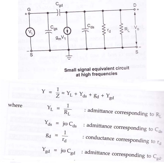
Voltage gain:
Input Admittance:

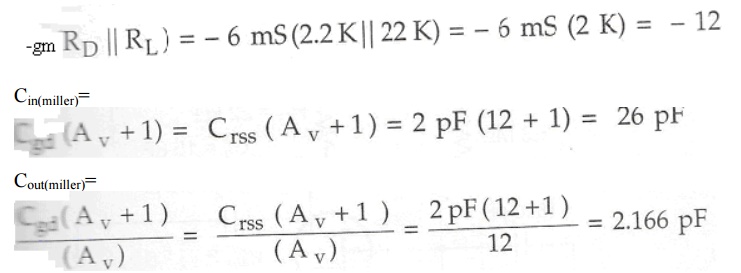
Input capacitance (Miller Effect):
This
increase in input capacitance Ci over the capacitance from gate to
source is called Miller effect.
This
input capacitance affects the gain at high frequencies in the operation of
cascaded amplifiers. In cascaded amplifiers, the output from one stage is used
as the input to a second amplifier. The input impedance of a second stage acts
as a shunt across output of the first stage and Rd is shunted by the
capacitance Ci.
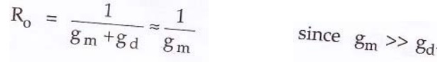
Output Admittance:
From
above figure, the output impedance is obtained by looking into the drain with
the input voltage set equal to zero. If Vi = 0 in figure, r d
,Cds and Cgd in parallel. Hence the output admittance
with RL considered external to the amplifier is given by

2. Common Drain Amplifier at High
Frequencies:
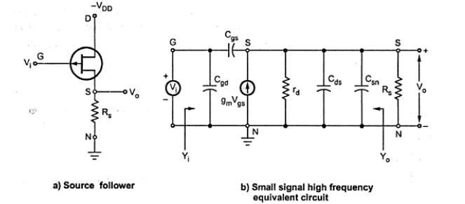
Fig.
Common Drain Amplifier Circuit & Small signal equivalent circuit at high
frequencies
Voltage gain:
The
output voltage Vo can be found from the product of the short circuit
and the impedance between terminals S and N. Voltage gain is given by,
Input Admittance:
Input
Admittance Yi can be obtained by applying Miller’s theorem to Cgs.
It is
given by,
Output Admittance:
Output
Admittance Yo with Rs considered external to the
amplifier, it is given by
At low
frequencies, output resistance Ro is given by,
3. Frequency Response of Common
Source Amplifier:
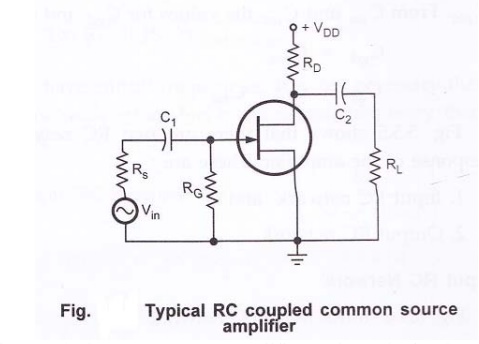
Let us
consider a typical common source amplifier as shown in the above figure.
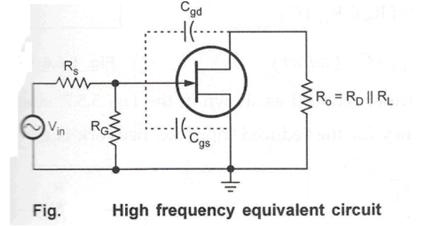
From
above figure, it shows the high frequency equivalent circuit for the given
amplifier circuit. It shows that at high frequencies coupling and bypass
capacitors act as short circuits and do not affect the amplifier high frequency
response. The equivalent circuit shows internal capacitances which affect the
high frequency response.
Using
Miller theorem, this high frequency equivalent circuit can be further
simplified as follows:
The
internal capacitance Cgd can be splitted into Cin(miller)
and Cout(miller) as shown in the following figure.
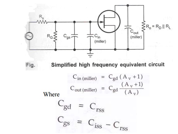
From
simplified high frequency equivalent circuit, it has two RC networks which
affect the high frequency response of the amplifier. These are,
·
Input RC network
·
Output RC network
Input RC network:
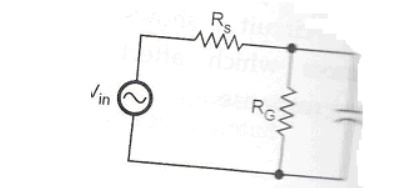
Fig.
Input RC network
From
above figure,
This
network is further reduced as follows since Rs<< RG
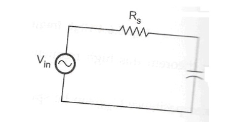
Fig.
Reduced input RC network
The
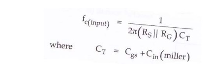
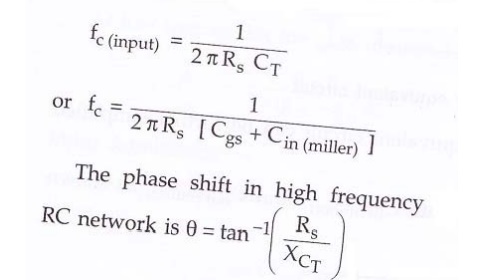
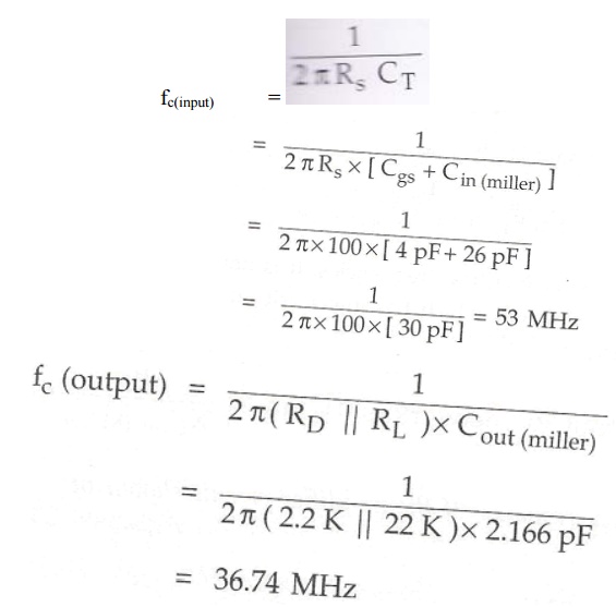
critical frequency for the reduced input RC network is,
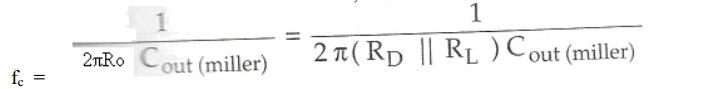
Output RC network:
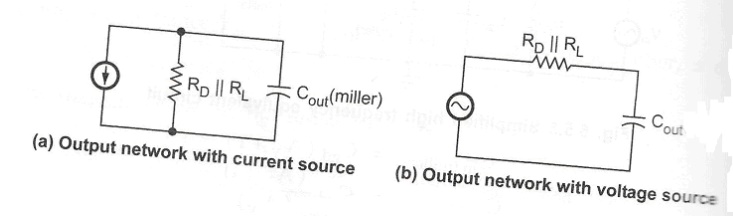
Fig.
Output RC network
The
critical frequency for the above circuit is,
It is not
necessary that these frequencies should be equal. The network which has lower
critical frequency than other network is called dominant network.
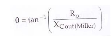
The phase
shift in high frequency is
Problem:
Determine
the high frequency response of the amplifier circuit shown in the following
figure.
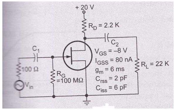
Solution:
Before
calculating critical frequencies it is necessary to calculate mid frequency
gain of
the given
amplifier circuit. This is required to calculate Cin(miller) and Cout(miller).
Av
= -gmRD
Here RD
should be replaced by RD || RL Av=
Cgs
= Ciss – Crss = 4pF
Now
analyze the input and output network for critical frequency,
The above
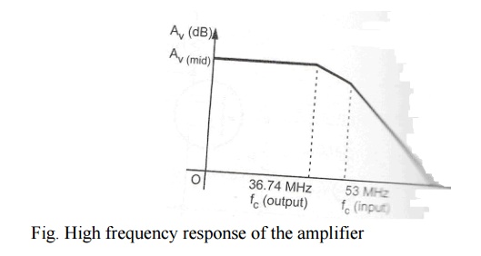
analysis shows that the output network produces the dominant higher critical
frequency. High frequency response of the given amplifier is shown in the
following figure
Related Topics