Chapter: Electronic Circuits : Feed Back Amplifiers
D.C. Analysis of Emitter Follower
The d.c. analysis of an emitter follower is made in the same way as the voltage divider bias circuit of a CE amplifier.
D.C. Analysis of Emitter Follower
The d.c. analysis of an emitter follower is made in the same way as
the voltage divider bias circuit of a CE amplifier. Thus referring to Fig. 1.9
above, we have,
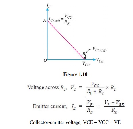
D.C.
Load Line. The d.c.
load line of emitter follower can be constructed by locating the two end points viz., IC(sat) and VCE(off).
(i)When the transistor is saturated, VCE = 0.

This locates the point A (OA = VCC÷
RE) of the d.c. load line as shown in Fig. 1.10.
(ii) When the transistor is cut off, IC =
0. Therefore, VCE(off) = VCC. This locates the point B
(OB = VCC) of the d.c.
load line.
By joining points A and B, d.c. load line AB is
constructed.
Study Material, Lecturing Notes, Assignment, Reference, Wiki description explanation, brief detail
Electronic Circuits : Feed Back Amplifiers : D.C. Analysis of Emitter Follower |
Related Topics
Electronic Circuits : Feed Back Amplifiers