Chapter: Discrete Time Systems and Signal Processing : Digital Signal Processor
Core Architecture Of ADSP-21xx
CORE
ARCHITECTURE OF ADSP-21xx
ADSP-21xx
family DSP's are used in high speed numeric processing applications.
ADSP-21xx
architecture consists of Five Internal
Buses
·
Program Memory Address(PMA)
·
Data memory address (DMA)
·
Program memory data(PMD)
·
Data memory data (DMD) and Result (R)
·
Three Computational Units are
Arithmetic
logic unit (ALU)
Multiply-accumulate
(MAC)
Shifter
·
Two Data Address generators (DAG)
·
Program sequencer
·
On chip peripheral Options
·
Data Memory
·
Timer
·
Serial Port
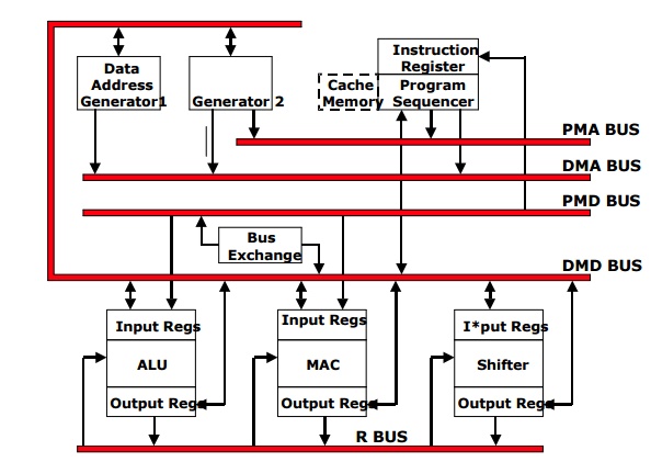
Block Diagram of Architecture
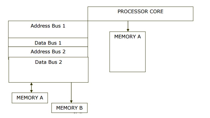
BUSES:
The
ADSP-21xx processors have five internal buses to ensure data transfer.
1.PMA and
DMA buses are used internally for addresses associated with Program and data
memory. The PMD and DMD are used for data associated with memory spaces. Off
Chip, the buses are multiplexed into a single external address bus and a single
external data bus. The address spaces are selected by the appropriate control
signal.
2.The
result (R) bus transfers the intermediate results directly between various
computational units.
3.PMA bus
is 14-bits wide allowing direct access of up to 16k words of code and data. PMD
bus is 24 bits wide to accommodate the 24 bit instruction width.
The DMA
bus 14 bits wide allowing direct access of up to 16k words of data.The DMD bus
is 16 bit wide.
4.The DMD
bus provides a path for the contents of any register in the processor to be
transferred to any other register or to any external data memory location in a
single cycle. DMA address comes from two sources. An absolute value specified
in the instruction code
(direct addressing) or the output
of DAG (Indirect addressing). The
PMD bus can
also be used
to transfer data
to and from
the computational units thro direct path or via PMD-DMD bus exchange
unit.
COMPUTATIONAL UNITS:
The
processor contains three -independent computational units. ALU, MAC
(Multiplier-accumulator) and the barrel shifter. The computational units
process 16-bit data directly. ALU is 16 bits wide with two 16 bit input ports
and one output port. The ALU provides a standard set of arithmetic and logic
functions.
ALU
Features
1. Add,
subtract, Negate, increment, decrement, Absolute value, AND, OR, EX-OR, Not
etc.
2. Bitwise
operators, Constant operators
3. Multi-precision
Math Capability
4. Divide
Primitives and overflow support.
MAC:
The MAC
performs high speed single-cycle multiply/add and multiply/subtract operations.
MAC has two 16 bit input ports and one 32 bit product output port. 32 bit
product is passed to a 40 bit adder/subtractor which adds or subtracts the new
product from the content of the multiplier result (MR). It also contains a 40
bit accumulator which provides 8 bit overflow in successive additions to ensure
that no loss of data occurs. 256 overflows would have to occur before any data
is lost. A set of background registers is also available in the MAC for
interrupts service routine.
SHIFTER:
The
shifter performs a complete set of shifting functions like logical and
arithmetic shifts (circular or linear shift) , normalization (fixed point to
floating point conversion), demoralization (floating point to fixed point
conversion) etc
ALU, MAC
and shifter are connected to DMD bus on one side and to R bus on other side.
All three sections contains input and output registers which are accessible
from the internal DMD bus. Computational operations generally take the operands
from input registers and load the result into an output register.
DATA ADDRESS GENERATORS (DAG):
Two DAG's
and a powerful program sequencer ensure efficient use of these computational
units. The two DAG's provides memory addresses when memory data is transferred
to or from the input or output registers. Each DAG keeps track of up to four
address pointers. Hence jumps, branching types of instructions are implemented
within one cycle. With two independent DAG's, the processor can generate two
address simultaneously for dual operand fetches.
DAG1 can
supply addresses to data memory only. DAG2 can supply addresses to either data
memory or program memory. When the appropriate mode bit is set in mode status
register (MSTAT), the output address of DAG1 is bit-reversed before being
driven onto the address bus. This feature facilitates addressing in radix-2 FFT
algorithm.
PROGRAM SEQUENCER:
The
program sequencer exchanges data with DMD bus. It can also take from PMD bus.
It supplies instruction address to program memory. The sequencer is driven by
the instruction register which holds the currently executing instruction. The
instruction register introduces a single level of pipelining into the program
flow. Instructions are fetched and loaded into the instruction register during
one processor cycle, and executed during the following cycle while the next
instruction is pre-fetched. The cache memory stores up to 16 previously
executed instructions. Thus data memory on PMD bus is more efficient because of
cache memory. This also makes pipelining and increase the speed of operations.
FEATURES OF ADSP-21xx PROCESSOR
1. 16 bit
fixed DSP microprocessor
2. Enhanced
Harvard architecture for three bus performance.
3. Separate
on chip buses for program and data memory.
4. 25 MIPS,
40 ns maximum instruction set 25Mhz frequency.
5. Single
cycle instruction execution i.e True instruction cycle.
6. Independent
computational units ALU, MAC and shifter.
7. On chip
program and data memories which can be extended off chip.
8. Dual
purpose program memory for instruction and data.
9. Single
cycle direct access to 16K × 16 of data memory.
10.
Single cycle direct access to 16K × 24 of program m
Related Topics