Chapter: Electronic Devices : Field Effect Transistors(FET)
Important short Questions and Answers: Field Effect Transistors(FET)
FIELD EFFECT TRANSISTORS
1. Define FET?
A field effect transistor (FET) is a three terminal
semiconductor device which can be used as an amplifier or switch. The three
terminals are Drain (D), Source (S), and Gate (G).
2. Define channel?
It is a
bar like structure which determines the type of FET. Different types of N
channel are FET and P channel FET.
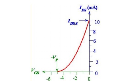
3. Draw the transfer characteristic for
n-channel depletion type MOSFET?
Transfer characteristic:
4. What do you understand by pinch off voltage
and out of voltage?
As the
reverse bias is further increased, the effective width of the channel
decreases, the depletion region or the space charge region widens, reaching
further into the channel and restricting the passage of electrons from the
source to drain. Finally at a certain gate to source voltage VGS = VP.
5. Why FET is called as “voltage operated
device”?
In FET
the output current, I D is controlled by the
voltage applied between gate and source (VGS).
Therefore FET is said to be voltage controlled device.
6.
Which
MOSFET is called as Normally ON MOSFET and NORMALLY OFF MOSFET? Why?
This is
just one type of MOSFET, called 'normally
-off' because it is only the application of a positive gate voltage above
the critical voltage which allows it to pass current between source and
drain.Another type of MOSFET is the 'normally-on',
which has a conductive channel of less heavily doped n-type material between the source and drain electrodes.
7. Compare
BJT and MOSFET
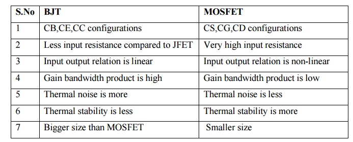
BJT
1 CB,CE,CC configurations
2 Less input resistance compared to JFET
3 Input output relation is linear
4 Gain bandwidth product is high
5 Thermal noise is more
6 Thermal stability is less
7 Bigger size than MOSFET
MOSFET
1
CS,CG,CD configurations
2 Very
high input resistance
3 Input
output relation is non-linear
4 Gain
bandwidth product is low
5 Thermal
noise is less
6 Thermal
stability is more
7 Smaller
size
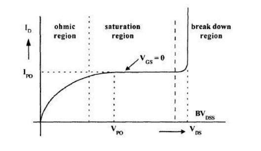
8. Sketch the ohmic region in drain
characteristics of JFET? Drain characteristics:
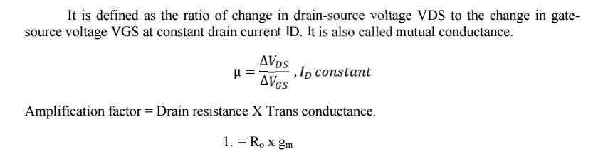
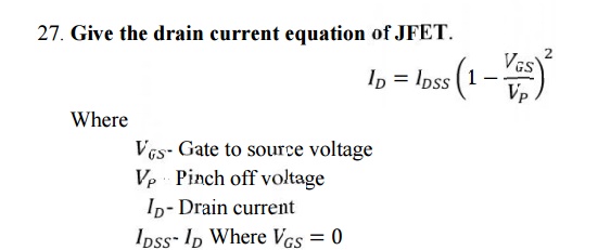
9. Define Amplification factor in JFET?
10.What are the advantages of FET over BJT?
·
In FET input resistance is high compared to BJT
Construction is smaller than BJT.
· Less
sensitive to changes in applied voltage
· Thermal
stability is more and Thermal noise is much lower Thermal runaway does not
exist in JFET
11. Comparison between JFET and BJT.
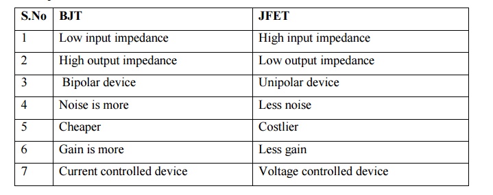
BJT
1 Low input impedance
2 High output impedance
3 Bipolar device
4 Noise is more
5 Cheaper
6 Gain is more
7 Current controlled device
JFET
1 High input impedance
2 Low output impedance
3 Unipolar device
4 Less noise
5 Costlier
6 Less gain
7 Voltage controlled device
12.
What are
the important features of FET?
·
The parameters of FET are temperature dependent. In
FET, as temperature increases drain resistance also increases, reducing the
drain current. Thus unlike BJT, thermal runaway does not occur with FET. Thus
we can say FET is more temperature stable.
·
FET has very high input impedance. Hence FET is
preferred in amplifiers. It is less noisy.
·
Requires less space.
·
It exhibits no offset voltage at zero drain
current.
13.
Comparison
between JFET and MOSFET.
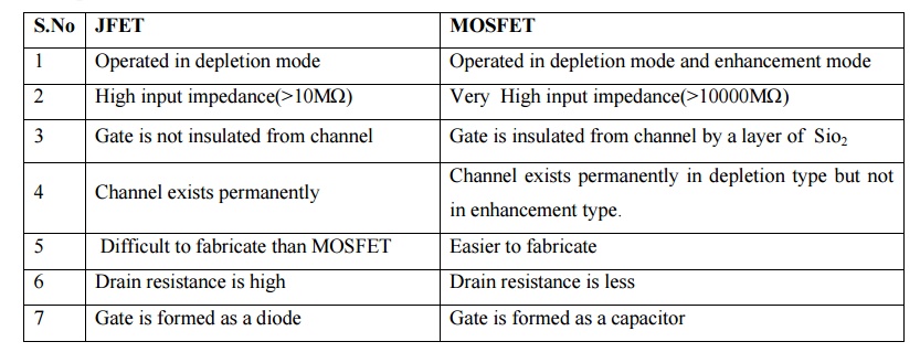
JFET
1 Operated in depletion mode
2 High input impedance(>10MΩ)
3 Gate is not insulated from channel
4 Channel exists permanently
5 Difficult to fabricate than MOSFET
6 Drain resistance is high
7 Gate is formed as a diode
MOSFET
1
Operated in depletion mode and enhancement mode
2
Very High input impedance(>10000MΩ)
3 Gate is
insulated from channel by a layer of
Sio2
4 Channel
exists permanently in depletion type but not in enhancement type.
5 Easier
to fabricate
6 Drain
resistance is less
7 Gate is
formed as a capacitor
14. Explain the biasing of JFET?
Input is
always reverse biased and output is forward biased. (Note: In transistor input
is forward biased and output is reverse biased).
15. Define Drain resistance.
It is the
ratio of change in Drain – source voltage (∆VDS) to the change in
Drain current (∆ID) at constant gate source voltage (VGS).
16. Define Tran’s conductance?
It is the
ratio of change in drain current (∆ID) to the change in Gate –
Source Voltage (∆VGS) at constant Drain – Source voltage (VDS).
17. Write the advantages of JFET?
Input
impedance of JFET is very high.
This
allows high degree of Isolation between the Input and Output circuit. Current
carriers are not crossing the junction hence noise is reduced drastically
18.
List the
JFET parameters?
A.C drain
resistance (rd) Trans conductance (gm) Amplification
factor (µ)
19.
Explain
the depletion node of operation in MOSFET?
When the
gate is at negative bias, the thickness of the depletion layer further
increases owing to the further increase of the induced positive charge. Thus
the drain current decreases, as the gate is made more negative. This is called
depletion mode of operation.
20. Explain the term Drain in FET?
The drain
is the terminal through which the current leaves the bar. Convention current
entering the bar is designated as ID.
21. Define the term Gate in FET?
The gate
consists of either P+ or N+ impurity regions, heavily
doped and diffused to the bar. This region is always reverse biased and in
fact, controls the drain current ID.
22.
Write the
relative disadvantages of an FET over that of a BJT?
1. The gain
bandwidth product in case of a FET is low as compared with a BJT.
2. The
category, called MOSFET, is extremely sensitive to handling therefore
additional precautions have to be considered while handling.
23.
Mention
the methods used for biasing circuits in FET?
Self-bias
and Potential divider bias.
24.
Explain
the term MOSFET?
In the
insulated gate FET, conductivity is controlled by the potential on the
insulated metal plate lying on the top of the channel the insulated gate field
effect transistor is often called metallic oxide semiconductor FET.
25.
Mention
the three regions that are present in the drain source characteristics of JFET?
·
Saturation region
·
Break down region
·
Ohmic region
26.
List the
characteristics of JFET.
·
Drain characteristics
·
Transfer characteristics.
28. Why MOSFET is called IGFET?
MOSFET is
constructed with gate terminal insulated from the channel. So it is also called
as insulated gate FET or IGFET.
29. Comparison between JFET and MOSFET
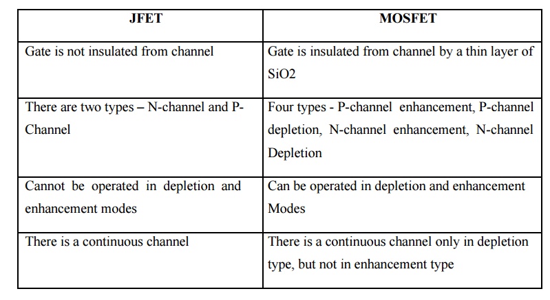
JFET
Gate is
not insulated from channel
There are
two types – N-channel and P-Channel
Cannot be
operated in depletion and enhancement modes
There is
a continuous channel
MOSFET
Gate is
insulated from channel by a thin layer of SiO2
Four
types - P-channel enhancement, P-channel depletion, N-channel enhancement,
N-channel Depletion
Can be
operated in depletion and enhancement Modes
There is
a continuous channel only in depletion type, but not in enhancement type
30. Compare P channel and N channel JFET.
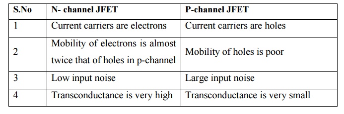
N-
channel JFET
1 Current carriers are electrons
2 Mobility of electrons is almost twice
that of holes in p-channel
3 Low input noise
4 Transconductance is very high
P-channel
JFET
1 Current
carriers are holes
2
Mobility of holes is poor
3 Large
input noise
4
Transconductance is very small
Related Topics