Chapter: Electronic Circuits : Frequency Analysis of BJT and MOSFET Amplifiers
Important Short Questions and Answers: Frequency Analysis of BJT and MOSFET Amplifiers
FREQUENCY ANALYSIS OF BJT AND
MOSFET AMPLIFIERS
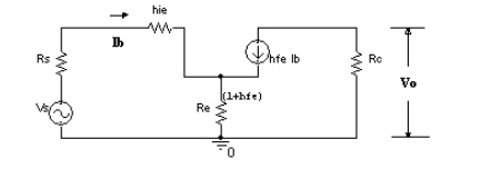
1. Draw the low frequency simplified h-parameter
model of an amplifier with a un bypassed emitter resistor.
2. Why an NPN transistor has a better high
frequency response than the PNP transistor?
An NPN
transistor has a better frequency response than the PNP transistor because the
mobility of electron is more and capacitive effect is less.
3. Define fT and f.
Unity
gain frequency (fT) or frequency parameter. It is defined as the
frequency at which the common emitter shirt circuit current gain has dropped to
unity and is denoted by the symbol (fT)
4. Beta cut-off frequency (fT).
It is
defined as the high frequency at which -of a CE transistor drops to 0.707 or
3dB from its lower frequencies
5. What is the need for having a high value of fT?
Bandwidth
of the amplifier is directly proportional to fT. Hence tp have
larger bandwidth, the value of fT should be high.
6. Why N-channel FET’s have a better response than
P-channel FET’s?
N-channel
FET has a better high frequency response than P-channel FET due to the
following
reason.
a. Mobility
of electrons is large in N-channel FET whereas the mobility of holes is poor in
P-channel FET
b. The input
noise is less in N-channel FET that that of the P-channel FET
c. The
transconductance is larger in N-channel FET that that of P-channel FET
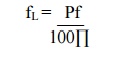
7. Write the relation between the sag and lower cutoff
frequency?
fH
= 2.2 / (2tr) = 0.35/tr
8. What is dominant network?
In high
frequency analysis of an amplifier, the network having lower critical frequency
is called dominant network.
9. What is the function of Miller input
capacitance of an amplifier?
The
Miller input capacitance of an amplifier is a function of Bypass capacitor.
10. What is the use of source bypass capacitor in CS
amplifier?
Source
bypass capacitor in CS amplifier is used for improving the voltage gain.
11.
Give two
advantages of common source FET amplifier?
a. Good
voltage gain
b. High
input impedance.
12.
What are
the advantages of representation of gain in decibels?
a. In
multistage amplifier, it permits to add individual gains of the stages to
calculate overall gain.
b. It allows
us to denote, both very small as well as very large quantities of linear scale
by considerably small figures.
13.
Write the
relation between the sag and lower cut-off frequency.
The tilt
of sag in time t1 is given by
P = Y of tilt
f = input
signal frequency
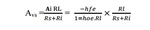
14. Give the voltage gain for CE configuration
including source resistance.
15. Why thermal runaway is not there in
MOSFETs?
MOSFET is
temperature dependent. In MOSFET, as temperature increases drain resistance
also increases’, reducing the drain current. So thermal runaway does not occur
in MOSFET.
16. Define transconductance?
The
change in the drain current due to change in gate to source voltage can be
determined using the transconductance factor gm. ∆Id=gm ∆VGS
17. Define emitter bypass capacitor?
An
emitter bypass capacitor CE is connected in parallel with the emitter
resistance, REto provide a low reactance path to the amplified ac signal. If it
is not inserted, the amplified ac signal passing through REwill cause a voltage
drop across it. This will reduce the output voltage, reducing the gain of the
amplifier.
18. Define coupling capacitor?
The
coupling capacitor cs, couples the output of the amplifier to the
load or to the next stage of the amplifier. It blocks dc and passes only ac
part of the amplified signal.
19. Define current gain
The ratio
of output current to input current is called current gain, AI, of
the amplifier. AI= I2 / I1.
20. Define voltage gain
The ratio
of output voltage to input voltage is called voltage gain AV , of
the amplifier. AV= V2/ V1
21.
Define
benefits of h-parameter.
• Real
numbers at audio frequencies
• Easy to
measure
• Can be
obtained from the transistor static characteristic curves
• Convenient
to use in circuit analysis and design.
• Most of
the transistor manufacturers specify the h-parameter.
.
22.
What are
the techniques used to improve input impedance.
• Using
direct coupling (Darlington connection)
• Using
Bootstrap techniques
23. Why the Darlington connection is not possible for
more number of stages?
In
Darlington connection of two transistors, emitter of the first transistor is
directly connected to the base of the second transistor. Because of direct
coupling dc output current of the first stage is (1+hfe)Ib1. If Darlington
connection for n stage is (1+hfe)n times Ib1. Due to very large
amplification factor even tow stage Darlington connection has large output
current and output stage may have to be a power stage. As power amplifiers are
not used in the amplifier circuits it is not possible to use more than two
transistors in the Darlington connection.
24. Briefly explain why dominant pole high
frequency compensation method used in amplifiers.
•
As the noise frequency components are outside the
smaller bandwidth, the noise immunity of the system improves.
•
Adjusting value of fd adequate phase
margin and stability of the system is assured.
25.
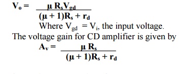
Write the
equation for the output voltage and voltage gain for CS amplifier.
The
output voltage is given by
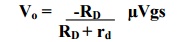
Where µ
is the amplification factor,
Rd
is the drain resistance
Vgs
= Vi, the input voltage
The
voltage gain for CS amplifier is given by
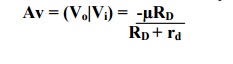
26. Write the equations for the output voltage and
voltage gain for CD amplifier.
The
output voltage is given by
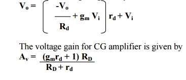
27. Write the equations for the output voltage
and voltage gain for CG amplifier.
The
output voltage is given by
Related Topics