Chapter: Electronic Devices : Field Effect Transistors(FET)
Field Effect Transistors(FET)
FIELD EFFECT TRANSISTORS
1 Introduction about FET
3 JFETs – Drain and Transfer characteristics 46
3 Pinch off voltage and its significance
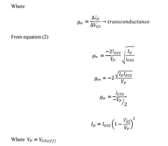
4 Current equations of FET
5 MOSFET
5.1 Symbol
5.2 D-MOSFET
5.3 E-MOSFET
5.3.1Symbol of E-MOSFET
5.3.2 Basic Construction
5.3.3 Operation
5.3.4 MOSFET- Characteristics
6 Channel length modulation
7 Threshold voltage
8 DUAL GATE MOSFET
9 FINFET
1 INTRODUCTION
Flow of current through the conducting region
controlled by an electric field. Hence the name field effect transistor (FET).
FET is
said to be a uni-polar device because current conduction is only by majority
carriers.
FET is
Voltage controlled device because its output characteristics are determined by
field which depends on the voltage applied.
It has
three terminals named as
·
Source (S)
·
Drain(D)
·
Gate(G)
1.1 CLASSIFICATION OF FET
FET is classified
into two types as follows
·
JFET (Junction Field Effect Transistor)
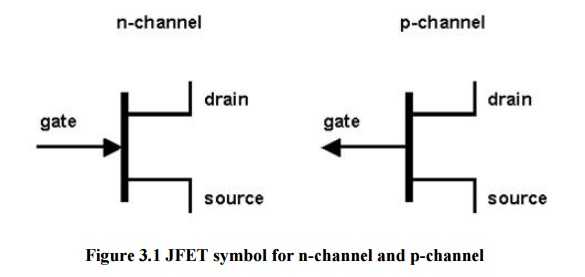
Ø n-channel
Ø p-channel
·
MOSFET(Metal Oxide Semiconductor (or) Insulated
Gate FET
Ø Depletion
type
ü n-channel
ü p-channel
Ø Enhancement
type
ü n-channel
ü p-channel
1.2Advantages of JFET over BJT
2. Operation
depends upon the flow of majority carriers only
3. It
exhibits a high input resistance (mega ohm) because gate constitute no current
but in BJT, base constitute a current.
4. Less
noisy.
5. It has
thermal stability
1.3 Disadvantages in JFET
1.Small
gain bandwidth product.
2 JFET [ Junction Field Effect Transistor ]
• JFET
can be used as a linear Resistor ≈ 0
• The
drain current is controlled by gate voltage applied at the gate VGS and
IG~0
Therefore it is termed as “ voltage controlled
device”.
2.1Types
1) N-channel
JFET
2) P-channel
JFET
2.2Symbol
2.3Construction
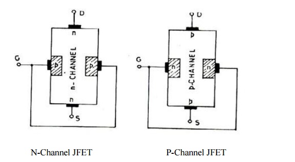
Figure 3.2 JFET construction for
n-channel and p-channel
·
It consists of N-type or P-type base which is made
of silicon.
·
Ohmic contacts made at the two ends of base called
source and drain.
Source(S):-
·
Connected to negative pole of battery.
·
Electrons enter the base through this terminal for
N-channel JFET.
Drain(D):-
·
Connected to postive pole of battery.
·
Electrons leave the base through this terminal for
N-channel JFET.
Gate(G):-
·
Heavily doped P-type silicon is diffused on both
sides of the N-channel base by which PN junction are formed.
·
These layers are joined together and called gate.
Channel:-
·
It is the space between the gate through which
majority carriers pass.
3 Operation of N-channel JFET
Transfer and Drain Characteristics:-
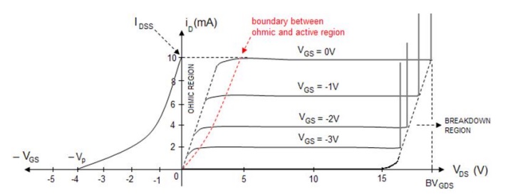
Figure 3.4 Transfer and Drain characteristics of
N-channel JFET
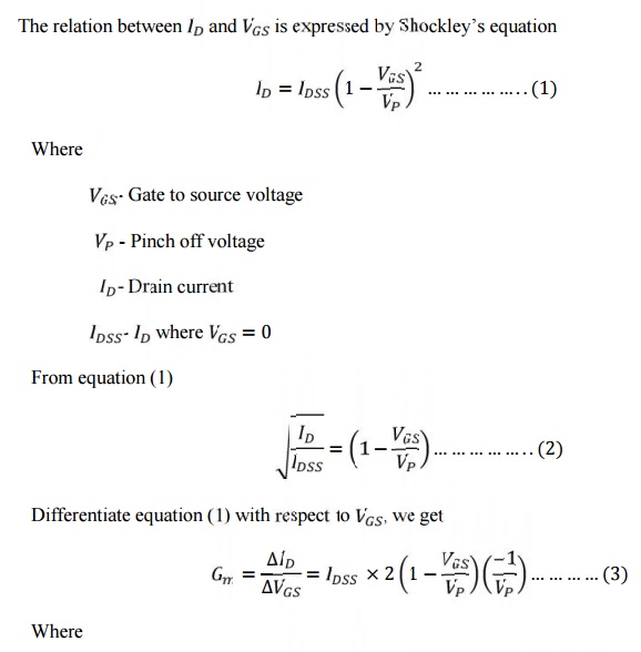
4 Current Equations
Applications
1) Used as
an amplifier
2) Used as
voltage variable resistor in operational amplifiers
3) Used in
mixer circuits in FM and TV receivers
5 MOSFET (Metal Oxide Semiconductor Field Effect
Transistor)
·
Like JFET, it has a sou rce, Drain and Gate.
·
It is also called IGFET (Insulated Gate FET)
because gate term inal is insulated from channel. Therefore it ha s extremely
high input resistance.
5.1 Types of MOSFET
It has
two types
Ø Depletio
n mode MOSFET
ü N-channel
ü P
-channel
Ø Enhance
ment mode MOSFET
ü N-channel
ü P
-channel
The
enhancement-type MOSFET is usually referred to as an E-MOSF ET, and the
depletion type, a D-MOSFET. The drain current in a MOSFET is controlled by the
ga te-source voltage VGS.
5.2 Depletion mode-MOSF ET
[D-MOSFET]
In
depletion mode of o peration the bias voltage on the gate reduc e the number of
charge carriers in the channel and therefore reduce the drain current ID.It
op erates in both depletion mode and enhancement mode.
5.2.1 Symbol
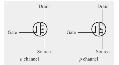
Figure 3.5 D -MOSFET symbol for n-channel and
p-channel
5.2.2 Construction
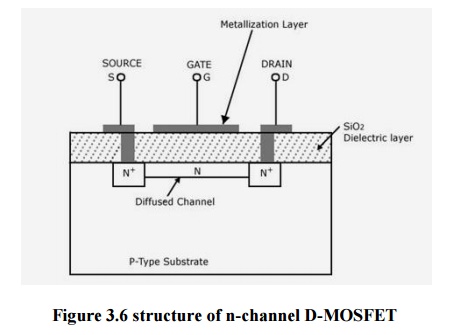
Figur e 3.6 structure of
n-channel D-MOSFET
·
It consists of lightly doped p-type substrate in
which two highly doped n-regions are diffused.
·
The source and drain terminals are connected
through metallic contacts to n-doped regions linked by an n-channel. The gate
is also connected to a m etal contact surface but remains insulated from the
n-channel by a very thin silicon dioxide (SiO2) layer. SiO2 is
a
particular type of insulator referred to as a dielectric that sets up opposing
(as revealed by the prefix di-) ele ctric fields within the dielectric when exp
osed to an externally applied field.
·
Then the thin layer of metal aluminium is formed
over the Sio2 layer. This metal overs the entire channel region a nd
it forms the gate(G).
5.2.3 Operation of N-channel D-MOSFET
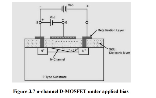
Figure 3.7 n-channel D-MOSFET under applied bias
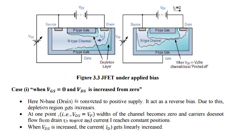
Case (i) “when and is increased from zero”
·
Here N-base (Drain) is connected to positive
supply. It act as a reverse bias. Due to this, depletion region gets increases.
·
Free electron from n-channel are attracted towards
positive potential of drain terminal. This establishes curren t through channel
flows from drain to source and denoted as IDSS.
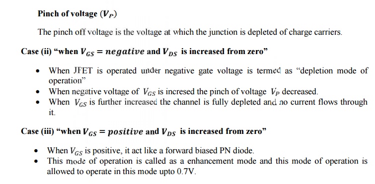
Pinch of voltage
The pinch
off voltage is th e voltage at which the junction is depleted of charge carriers.
Case (ii) “when and is increased from zero”
·
The negative charge on gate repels conduction
electrons from the c hannel and attract holes from the p-type substra te.
·
Due to this electron-ho le recombination occurs and
reduce the num ber of free electrons in the channel available f or conduction,
reducing Drain current (ID).
· When negative voltage of is incresed the pinch of voltage decreased.When is
further
increased the channel is fully depleted and no current flows through it.
·
The negative voltage on the gate deplete the
channel, the device is referred to as a depletion MOSFET.
Case (iii) “when and is increased from zero”
· Due to positive ,ad ditional electrons are
induced in the channel. Hence the conductivity
of the
channel increase s and current (ID) increases.
·
This mode of operation is called as a enhancement
mode and it is also called as dual mode MOSFET or ON-MOS FET.
5.2.4 Characteristics curve
Two types
· Drain characteristics
· Transfer characteristics
D-MOSFET’s
are biased to operate in two modes :depletion or enhancement mode.
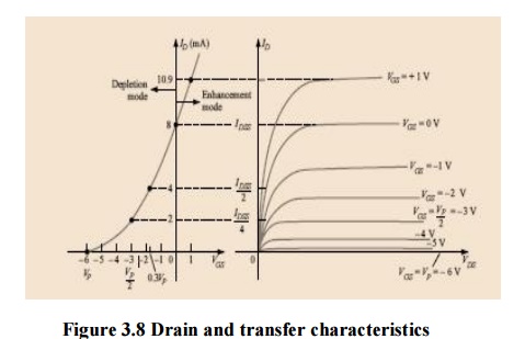
Figure 3.8 Drain and transfer characteristics
5.3 ENHANCEMENT- M ODE MOSFET
[E-MOSFET]
In this mode bias on th e gate increases the number
of charge carriers in the channel and increases the drain current (ID).
It operates only in the enhancement mode and has no
depletion mo de of operation.It has no physical channel.
5.3.1 Symbol of E-MOSFET
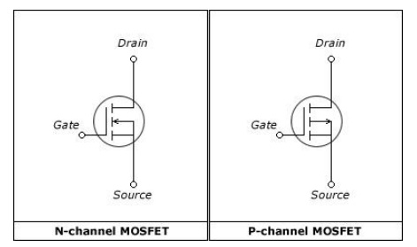
Figure 3.9 symbol of n-channel and p0 channel E-MOSFET
5.3.2 Basic Construction
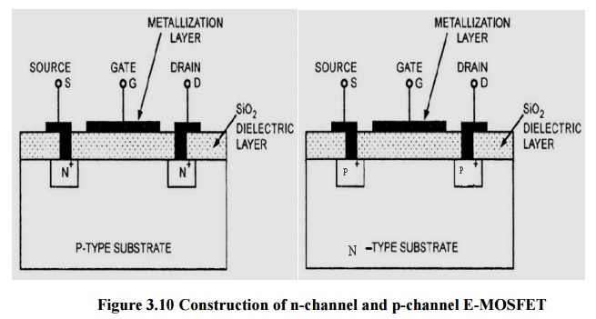
Figure 3.10 Co nstruction of
n-channel and p-channel E-M OSFET
In the
basic construction of the n-channel enhancement-type MOSFET, a slab of p-type
material is formed from a si licon base and is again referred to as the
substrate. As with the depletion-type MOSFET, the substrate is sometimes
internally connected to the source terminal, while in other cases a fourth lead
is made available for external control of its potential level.
The SiO2
layer is s till present to isolate the gate metallic platform from the region
between the drain and sour ce, but now it is simply separated from a section of
the p-type material.
In
summary, therefor e, the construction of an enhancement-type MOSFET is quite
similar to that of the depletion-type MOSFET, except for the absence of a
channel between the drain and source terminals.
5.3.3 Operation
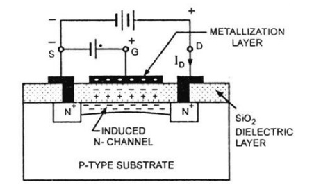
Figure 3. 11 N-channel E-MOSFET
under applied bias
· If VGS is set at 0 V and a voltage applied
between the drain an d source of the device, the absence of an n-c hannel (with
its generous number of free carriers) will result in a current of effectively z
ero amperes—quite different from the depletion- type MOSFET and JFET where ID -
IDSS .
·
It is not sufficient to have a large accumulation
of carriers (electrons) at the drain and source (due to the n-doped regions) if
a path fails to exist between the two. WithVDS some positive
voltage, VGS a t 0 V, and terminal SS directly connected to the
source, there are in fact two reverse-biased p-n junctions between the n-doped
regions and the p-substrate to oppose any significant flow between drain and
source.
·
When both VDS and VGS have
been set at some positive voltage greater than 0 V, establishing the drain and
gate at a positive potent ial with resp ect to the source. The positive
potential at the gate will pressure the holes (since like c harges repel) in
the p-substrate along the edge of the SiO2 layer to leave the area and enter
deeper regions of the p-substrate.
·
As VGS
is increased beyond the threshold level, the density of free carriers in the
induced channel will increase, resulting in an increased level of drain curre
nt. However, if we hold VGS constant and incr ease the level of VDS,
the drain current will eventually reach a saturation level as occ urred for the
JFET and depletion-type MO SFET.
·
The conductivity of th e channel is enhanced by the
positive bias voltage on the gate, the
device is
known as en hancement MOSFET. E-MOSFET’s are normally called as “OFF –
MOSFET”
5.3.4 Characteristics of E-MOSFET
Drain
characteristics curve
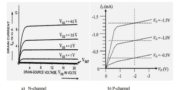
Figure 3.12 Drain characteristics
curve a) n-channel b ) p-channel
Transfer
characteristics curve
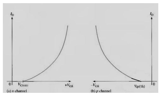
Figure 3.13 T ransfer
characteristics curve a) n-channel b) p-channel
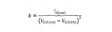
For
levels of VGS > VT, the drain current is related to
the applied gate-to-source voltage by the following nonlinear relationship:

Where,
k-constant depends upon type of MOSFET.
Again, it
is the squared term that results in the nonlinear (curved) relationship between
ID and VGS. The k term is a constant that is a function of the
construction of the device. The value of k can be determined from the following
equation where ID(on) and VGS(on) are the values for each at a particular point
on the characteristics of the device.
5.4 Applications:
1. Used in
digital VLSI circuits
2. Used as
amplifiers
3. Used in
computer memories
4. Used as
oscillator and in communication.
6 CHANNEL LENGTH MODULATION
One of
several short-channel effects in MOSFET scaling, channel length modulation
(CLM) is a shortening of the length of the inverted channel region with
increase in drain bias for large drain biases. The result of CLM is an increase
in current with drain bias and a reduction of output resistance. Channel length
modulation occurs in all field effect transistors, not just MOSFETs.
To
understand the effect, first the notion of pinch-off of the channel is
introduced. The channel is formed by attraction of carriers to the gate, and
the current drawn through the channel is nearly a constant independent of drain
voltage in saturation mode. However, near the drain, the gate and drain jointly
determine the electric field pattern. Instead of flowing in a channel, beyond
the pinch-off point the carriers flow in a subsurface pattern made possible
because the drain and the gate both control the current. In the figure at the
right, the channel is indicated by a dashed line and becomes weaker as the
drain is approached, leaving a gap of uninverted silicon between the end of the
formed inversion layer and the drain (the pinch-off region).
As the
drain voltage increases, its control over the current extends further toward
the source, so the uninverted region expands toward the source, shortening the
length of the channel region, the effect called channel-length modulation.
Because resistance is proportional to length, shortening the channel decreases
its resistance, causing an increase in current with increase in drain bias for
a MOSFET operating in saturation. The effect is more pronounced the shorter the
source-to-drain separation, the deeper the drain junction, and the thicker the
oxide insulator.
In
bipolar devices a similar increase in current is seen with increased collector
voltage due to base-narrowing, known as the early effect. The similarity in
effect upon the current has led to use of the term "Early effect" for
MOSFETs as well, as an alternative name for "channel-length
modulation".
Channel
length modulation: the channel pinch-off point moves slightly away from drain
as .The effective c hannel length Leff reduces with .Electrons travel to
pinch-off point will be swept to drain by electric field.
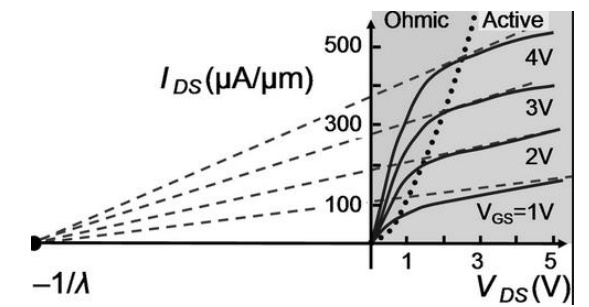
Figure
3.14 Effec t of channel length modulation due to the non-zero slope in
saturation region, resulting in a finite output resistance
For an
N-channel device the s lope of the curve in the saturation region ca n be
expressed by using the drain current ID given by
-------------
The
output resistance can be d etermined at the Q-point by
-------------
The output resistance is an important factor in the analysis of small s ignal equivalent circuit of MOSFET.
7 THRESHOLD VOLTAGE
The
threshold voltage, commonly abbreviated as Vth or VGS (th),
of a field-effect transistor (FET) is the minimum gate-to-source v oltage
differential that is needed to create a conducting path between the source and
drain terminals.
At
gate-to-source voltages abo ve the threshold voltage (VGS > Vth)
but stil l below saturation (less than "fully on", (VGS -
Vth) > VDS), the transistor is in its 'linear region',
also known as ohmic
mode,
where it behaves like a voltage-controlled variable resistor.
In
n-channel enhancement-mode devices, a conductive channel does not e xist
naturally within the transistor, and a positive gate -to-source voltage is
necessary to create one. The positive voltage attracts free-floating electrons
within the body towards the gate, forming a conductive channel. But first,
enough electrons must be attracted near the gate to counter the dopant ions
added to the body of the FET; this forms a region with no mobile carriers
called a depletion re gion, and the voltage at which this occurs is the
threshold voltage of the FET. Further gate-to-source voltage increase will
attract even more electrons to wards the gate which are able to create a c
onductive channel from source to drain; this process is called inversion.
In
contrast, n-channel depletion-mode devices have a conductive channel n aturally
existing within the transistor. Accordingly, the term 'threshold voltage' does
not readily ap ply to turn such devices 'on', but is used instead to denote the
voltage level at which the channel is wide enough to allow electrons to flow
easily. This ease-of-flow threshold also applies to p-c hannel depletion-mode
devices, in which a positive v oltage from gate to body/source creates a
depletion layer by forcing the positively charged holes away from the
gate-insulator/semiconductor interface, leaving exposed a carrier-free region o
f immobile, negatively charged acceptor ions.
8 DUAL GATE MOSFETS
MOSFET
can be provided with two gates. Both gates can be used indep endently to
control the drain current or the channel ressistance. Dual gate MOSFET are
normally of the n-channel depletion type. The dual-gate MOSFET has a tetrode
configuration, where both gate s control the current in the device.
8.1 Symbol and Construction
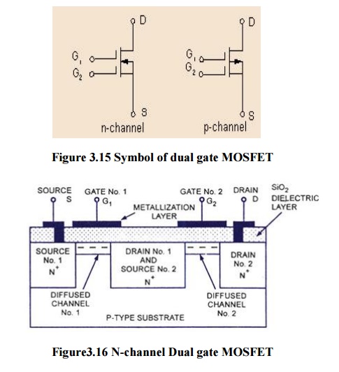
The
output signal of the dual gate MOSFET is approximately proportional to the
PRODUCT of the input voltages:
8.2 Applications :
·
This makes this device suitable for applications
where the multiplication of signals is required.E.g. modulatio n, mixing,
demodulation, automatic gain con trol etc.
·
It is also used as signal switch
· One gate serves as in put for the signal to
be amplified or transf erred, the other as the control input. The advantage is,
that the signal and the control voltag e are fully separated.
9 FINFET
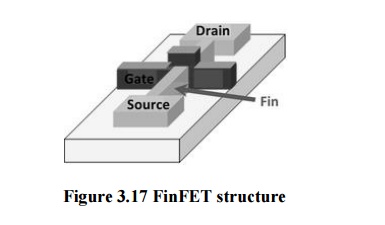
Figure 3.17 FinFET structure
The
distinguishing characteristic of the FinFET is that the conducting ch annel is
wrapped by a thin silicon "fin", which forms the body of the device.
The thickness of t he fin (measured in the direction from source to drain )
determines the effective channel length of the device.
The
"Omega FinFET" design is named after the similarity between the Greek
letter omega (Ω) and the shape in which the gate wra ps around the source/drain
structure. It has a gate delay of just 0.39 picosecond (ps) for the N-type
transistor and 0.88 ps for the P-type. Fin FET can also have two electrically
independent gates, which gives circuit designers more flex ibility to design
with efficient, low-power gates.
Applications:
The
double gate FinFETs which are driven independently are used to construct low
power logic gates, single transistor mixer s and SRAMs
Related Topics