Chapter: RF and Microwave Engineering : Two Port RF Networks : Circuit Representation
Two Port RF Networks - Circuit Representation
TWO PORT RF NETWORKS – CIRCUITE REPRESENTATION
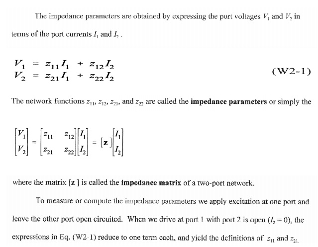
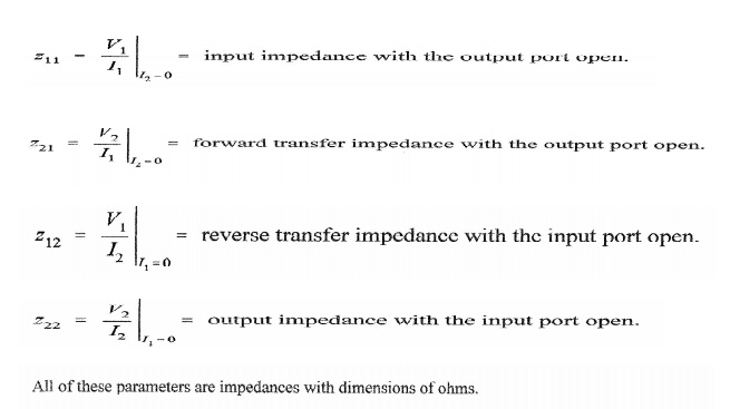
2. IMPEDANCE PARAMETERS
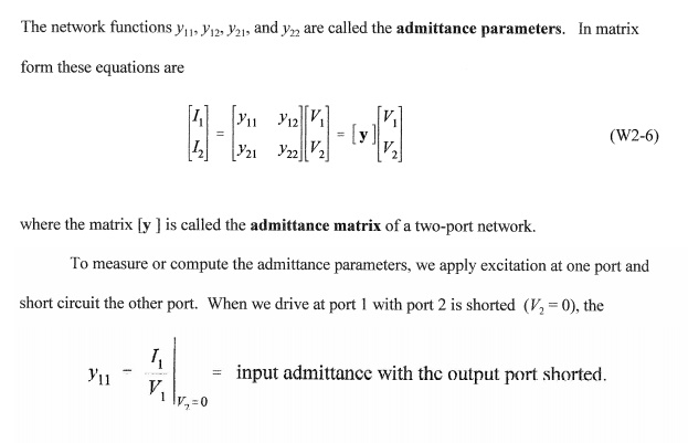
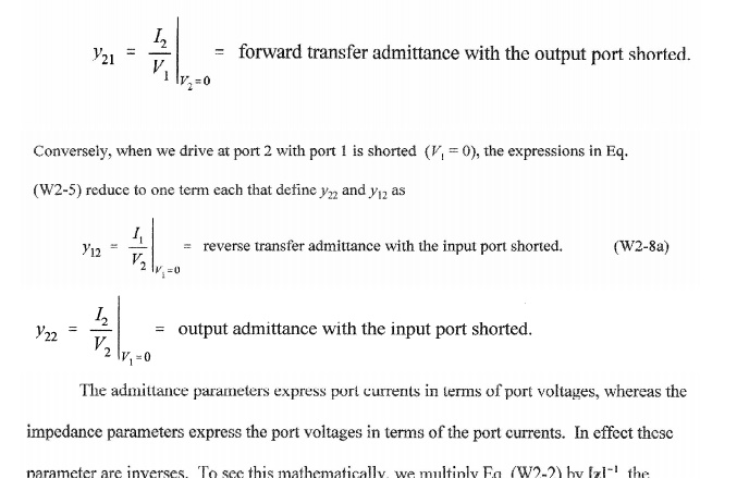
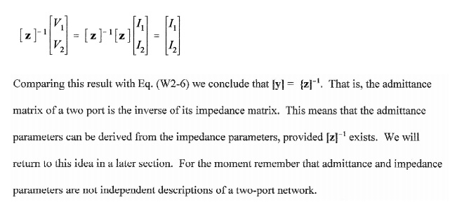
3. ADMITTANCE PARAMETERS
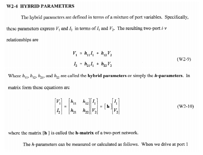
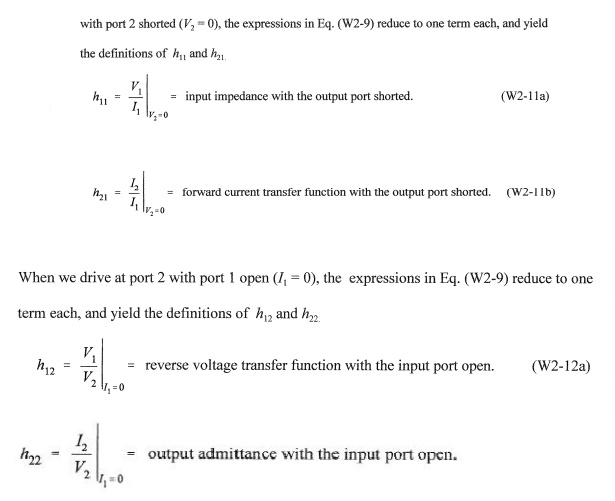
4. HYPRID PARAMETERS
5. ABCD PARAMETERS
6. HIGH FREQUENCY PARAMETER
7. FORMULATION OF S – PARAMETER
7.1. PROPERTIES OF S-PARAMETE
8. RECIPROCAL AND LOSS LESS NETWORKS
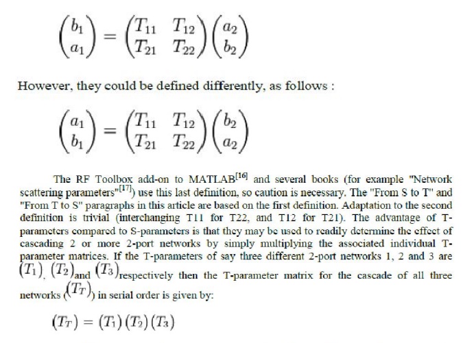
9. TRANSMISSION MATRIX
10. INTODUCTION TO COMPONENT BASICS
11. WIRE
12. RESISTOR
13. INDUCTOR
14. CAPACITOR
1. LOW FREQUENCY PARAMETERS:
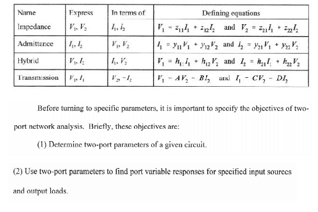
2. IMPEDANCE PARAMETERS
3. ADMITTANCE PARAMETERS

4. HYPRID PARAMETERS
5. ABCD PARAMETERS:
The ABCD-parameters are known variously as chain, cascade, or transmission line parameters. There are a number of definitions given for ABCD parameters, the most common

For reciprocal networks AD – BC =1 For symmetrical networks A = D . For networks which are reciprocal and lossless, A and D are purely real while B and C are purely imaginary.
This representation is preferred because when the parameters are used to represent a cascade of two-ports, the matrices are written in the same order that a network diagram would be drawn, that is, left to right. However, the examples given below are based on a variant definition
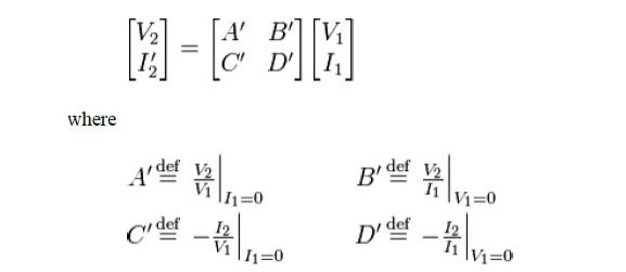
The negative signs in the definitions of parameters C’ and D’arise because I2’ is defined with the opposite sense to I2 , that is,I2’ = I2 . The reason for adopting this convention is so that the output current of one cascaded stage is equal to the input current of the next. Consequently, the input voltage/current matrix vector can be directly replaced with the matrix equation of the preceding cascaded stage to form a combined A’B’C’D’matrix.
The terminology of representing the parameters as a matrix of elements designated a11 etc as adopted by some authors[10] and the inverse parameters as a matrix of elements designated b11 etc is used here for both brevity and to avoid confusion with circuit elements.
6. HIGH FREQUENCY PARAMETER
The s parameter is called as high frequency parameter
7. FORMULATION OF S – PARAMETER
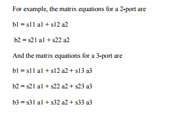
An n-port microwave network has n arms into which power can be fed and from which power can be taken. In general, power can get from any arm (as input) to any other arm (as output). There are thus n incoming waves and n outgoing waves. We also observe that power can be reflected by a port, so the input power to a single port can partition between all the ports of the network to form outgoing waves. Associated with each port is the notion of a "reference plane" at which the wave amplitude and phase is defined. Usually the reference plane associated with a certain port is at the same place with respect to incoming and outgoing waves. The n incoming wave complex amplitudes are usually designated by the n complex quantities an, and the n outgoing wave complex quantities are designated by the n complex quantities bn. The incoming wave quantities are assembled into an n-vector A and the outgoing wave quantities into an n-vector B. The outgoing waves are expressed in terms of the incoming waves by the matrix equation B = SA where S is an n by n square matrix of complex numbers called the "scattering matrix". It completely determines the behaviour of the network. In general, the elements of this matrix, which are termed "s-parameters", are all frequency-dependent.
For example, the matrix equations for a 2-port are
The wave amplitudes an and bn are obtained from the port current and voltages by the relations a = (V + ZoI)/(2 sqrt(2Zo)) and b = (V - ZoI)/(2 sqrt(2Zo)). Here, a refers to an if V is Vn and I In for the nth port. Note the sqrt(2) reduces the peak value to an rms value, and the sqrt(Zo) makes the amplitude normalised with respect to power, so that the incoming power = aa* and the outgoing power is bb*.
A one-port scattering parameter s is merely the reflection coefficient gamma, and as we have seen we can relate gamma to the load impedance zL = ZL/Zo by the formula gamma = (zL-1)/(zL+1).
Similarly, given an n by n "Z-matrix" for an n-port network, we obtain the S matrix from the formula S = (Z-I)(Z+I)^-1, by post-multiplying the matrix (Z-I) by the inverse of the matrix (Z+I). Here, I is the n by n unit matrix. The matrix of z parameters (which has n squared elements) is the inverse of the matrix of y parameters.
PROPERTIES OF S-PARAMETER
1) Zero diagonal elements for perfect matched network
For an ideal network with matched termination Sii=0, since there is no refiection from any port. Therefore under perfect matched condition yhe diagonal element of [s] are zero
2) Symmetry of [s] for a reciprocal network
The reciprocal device has a same transmission characteristics in either direction of a pair of ports and is characterized by a symmetric scattering matrix
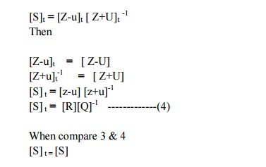
Sij = Sji ; i≠j Which results [S] t = [S]
For a reciprocal network with assumed normalized the impeadence matrix equation is [b]
= ( [z] + [u] )-1 ([z] – [u]) [a] -----------(1)
Where u is the unit matrix
S matrix equation of network is
[b] = [s] [a] ------------ (2)
Compare equ (1) & (2) [s] =([z]+[u])-1 ([z] – [u]) [R] = [Z] – [U]
[Q] = [Z] + [U]
For a reciprocal network Z matrix Symmetric
[R][Q] = [Q] [R]
[Q]-1 [R][Q][Q]-1 = [Q]-1[Q][R][Q]-1
[Q] -1[R] = [R][Q]-1
[Q] -1[R] [ S ] = [R][Q]-1 ------------(3) TRANSPOSE OS [s] IS NOW GIVEN AS
3) Unitary property of lossless network
For any loss less network the sum of product of each term of any one row or any one column of s matrix multiplied by its complex conjugate is unity
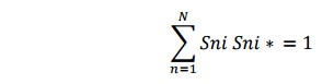
For a lossless N port devices the total power leaving N ports must be equal to total input to the ports
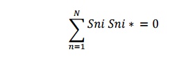
4) Zero property
It states that the sum of the product of any each term of any one row or any one column of a s matrix is multiplied by the complex conjucate of corresponding terms of any other row is zero
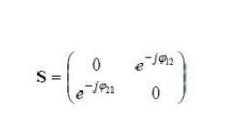
5) Phase shift propert
If any of the terminal or reference plane are mover away from the junction by an electric
distance βk, lk. each of the coefficient Sij involving K will be multiplied by the factor (e – jβk/k)
8. RECIPROCAL AND LOSS LESS NETWORKS:
1) Symmetry of [s] for a reciprocal network
The reciprocal device has a same transmission characteristics in either direction of a pair of ports and is characterized by a symmetric scattering matrix
Sij = Sji ; i≠j Which results [S] t = [S]
For a reciprocal network with assumed normalized the impeadence matrix equation is [b] = ( [z] + [u] )-1 ([z] – [u]) [a] -----------(1)
Where u is the unit matrix
S matrix equation of network is [b] = [s] [a] ------------(2)
Compare equ (1) & (2) [s] =([z]+[u])-1 ([z] – [u]) [R] = [Z] – [U]
[Q] = [Z] + [U]
For a reciprocal network Z matrix Symmetric [R] [Q] = [Q] [R]
[Q] -1[R][Q][Q]-1 = [Q]-1[Q][R][Q]-1 [Q] -1[R] = [R][Q]-1
[Q] -1[R] [ S ] = [R][Q]-1
9. TRANSMISSION MATRIX
The Scattering transfer parameters or T-parameters of a 2-port network are expressed by the T-parameter matrix and are closely related to the corresponding S-parameter matrix. The Parameter matrix is related to the incident and reflected normalized waves at each of the ports as follows:
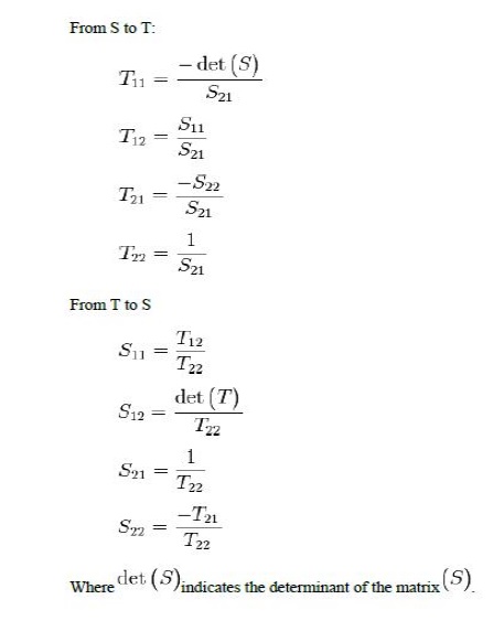
equivalent cascaded S-parameters, which are usually required, is not trivial. However once the operation is completed, the complex full wave interactions between all ports in both directions will be taken into account. The following equations will provide conversion between S and T parameters for 2- port networks.
10. INTODUCTION TO COMPONENT BASICS:
WIRE
CAPACITOR
INDUCTOR
RESISTOR
11. WIRE:
RF Cable Assembly is a quality manufacturer of standard and custom cable assemblies and electromechanical wiring harnesses for medical, computer, LAN, RF, automotive, monitoring and communications equipment. We can build custom cables to meet your requirements, whether standard or special.
Complete product design, tooling design and fabrication, materials processing and selection, product manufacture, assembly, testing and packaging are available in our San Diego facility.
All our assembly and soldering technicians have been trained to the requirements of IPC/EIA J-STD-001 and IPC/WHMA-A-620. By creating and using hand tools and assembly jigs designed for their tasks and using them in our documented production processes, we produce quality with repeatability.
12. RESISTOR:
The H, Y, Z and ABCD parameters are difficult at microwave frequencies due to the following reasons. (i)Equipment is not readily available to measure total voltage and total current at the ports of the network.
(ii) Short circuit and open circuit are difficult to achieve over a wide range of frequencies.
(iii) Presence of active devices makes the circuit unstable for short or open circuit.
Therefore microwave circuits are analyzed using scattering or S parameters which linearly relate the reflected wave amplitude with those of incident waves.
13. :INDUCTOR:
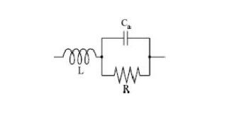
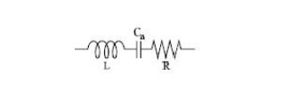
This inductance is exacerbated by the leads of the capacitor, which often dominate the inductance. The inductive parasitics are lumped into a single inductor Ls in series with the capacitor. The finite conductivity of the plates and the leads also results in some series loss, modeled by Rs (sometimes labeled ESR, or effective series resistance). Unless a capacitor is fabricated in a vacuum, the dielectric material that separates the plates also has loss (and resonance), which is usually modeled by a large shunt resistance, Rdi. Furthermore, when a capacitor is soldered onto a PCB, there is parasitic capacitance from the solder pads to the ground plane, resulting in the capacitors, Cp, in the equivalent model. In a like manner, every inductor also has parasitics, as shown in the equivalent circuit model (Fig. 4), which limit operating frequency range. The series resistance, Rx, is due to the winding resistance, and the capacitance Cx models the distributed turn-to-turn capacitance of the windings. The inductorself resonates at a frequency of approximately 1/ √ LCx and has a quality factor Q = ωL/Rx. When the inductor is soldered onto the PCB, there is an additional capacitance to ground modeled by Cp, which lowers the self-resonant frequency to 1/ p L(Cx + Cp/2).
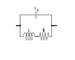
14: CAPACITOR:
now you have probably simulated your circuits with ideal passive components (inductors, capacitors, resistors), but real circuit components are far from ideal. Consider, for instance, a capacitor, which has an equivalent circuit model shown in Fig. 2. The model has many parasitic components which only become relevant at high frequencies. A plot of the impedance of the capacitor, shown in Fig. 3, shows that in addition to the ideal behavior, the most notable difference is the self-resonance that occurs for any real capacitor. The selfresonance is inevitable for any real capacitor due to the fact that as AC currents flow through a capacitor, a magnetic field is also generated by the capacitor, which leads to inductance
Related Topics