Chapter: Digital Principles and System Design : Design With MSI Devices
Design With MSI Devices
DESIGN WITH MSI DEVICES
MULTIPLEXERS
Many tasks in
communications, control, and computer systems can be performed by combinational
logic circuits. When a circuit has been designed to perform some task in one
application, it often finds use in a different application as well. In this
way, it acquires different names from its various uses. In this and the
following sections, we will describe a number of such circuits and their uses.
We will discuss their principles of operation, specifying their MSI or LSI
implementations. One common task is illustrated in Figure 12. Data generated in
one location is to be used in another location; A method is needed to transmit
it from one location to another through some communications channel. The data
is available, in parallel, on many different lines but must be transmitted over
a single communications link. A mechanism is needed to select which of the many
data lines to activate sequentially at any one time so that the data this line
carries can be transmitted at that time.This process is called multiplexing.An
example is the multiplexing of conversations on the telephone system. A number
of telephone conversations are alternately switched onto the telephone line
many times per second. Because of the nature of the human auditory system,
listeners cannot detect that what they are hearing is chopped up and that other
people‘s conversations are interspersed with their own in the transmission
process.
Needed at the other end of the communications
link is a device that will undo the multiplexing: a demultiplexer. Such a
device must accept the incoming serial data and direct it in parallel to one of
many output lines. The interspersed snatches of telephone conversations, for
example, must be sent to the correct listeners.
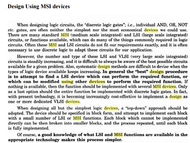
A digital multiplexer is a circuit with 2n
data input lines and one output line. It must also have a way of determining
the specific data input line to be selected at any one time. This is done with
n other input lines, called the select or selector inputs, whose function is to
select one of the 2n data inputs for connection to the output. A circuit for n
= 3 is shown in Figure 13. The n selector lines have 2n = 8 combinations of
values that constitute binary select numbers
Multiplexer with eight
data inputs
Multiplexers as
General-Purpose Logic Circuits
It is clear from Figures 13 and 14 that the
structure of a multiplexer is that of a two-level AND-OR logic circuit, with
each AND gate having n + 1 inputs, where n is the number of select inputs. It
appears that the multiplexer would constitute a canonic sum-of-products
implementation of a switching function if all the data lines together represent
just one switching variable (or its complement) and each of the select inputs
represents a switching variable.
Let‘s work backward
from a specified function of m switching variables for which we have written a
canonic sum-of-products expression. The size of multiplexer needed (number of
select inputs) is not evident. Suppose we choose a multiplexer that has m - 1
select inputs, leaving only one other variable to accommodate all the data
inputs.We write an output function of these select inputs and the 2m–1 data
inputs Di. Now we plan to assign m - 1 of these variables to the select inputs;
but how to make the assignment?4 There are really no restrictions, so it can be
done arbitrarily. The next step is to write the multiplexer output after
replacing the select inputs with m - 1 of the variables of the given function.
By comparing the two expressions term by term, the Di inputs can be determined
in terms of the remaining variable.
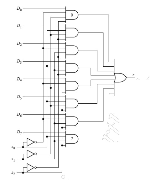
Demultiplexers
The demultiplexer shown
there is a single-input, multiple-output circuit. However, in addition to the
data input, there must be other inputs to control the transmission of the data
to the appropriate data output line at any given time. Such a demultiplexer
circuit having eight output lines is shown in Figure 16a. It is instructive to
compare this demultiplexer circuit with the multiplexer circuit in Figure 13.
For the same number of control (select) inputs, there are the same number of
AND gates. But now each AND gate output is a circuit output. Rather than each
gate having its own separate data input, the single data line now forms one of
the inputs to each AND gate, the other AND inputs being control inputs.
When the word formed by the control inputs
C2C1C0 is the binary equivalent of decimal k, then the data input x is routed
to output Dk. Viewed in another way, for a demultiplexer with n control inputs,
each AND gate output corresponds to a minterm of n variables. For a given
combination of control inputs, only one minterm can take on the value 1; the
data input is routed to the AND gate corresponding to this minterm. For
example, the logical expression for the output D3 is xC2'C1C0. Hence, when
C2C1C0 = 011, then D3 = x and all other Di are 0.
The complete truth
table for the eight-output demultiplexer.
A demultiplexer circuit
(a) and its truth table (b).
DECODERS AND ENCODERS
The previous section began by discussing an
application: Given 2n data signals, the problem is to select, under the control
of n select inputs, sequences of these 2n data signals to send out serially on
a communications link. The reverse operation on the receiving end of the communications
link is to receive data serially on a single line and to convey it to one of 2n
output lines. This again is controlled by a set of control inputs. It is this
application that needs only one input line; other applications may require more
than one.We will now investigate such a generalized circuit.
Conceivably, there
might be a combinational circuit that accepts n inputs (not necessarily 1, but
a small number) and causes data to be routed to one of many, say up to 2n,
outputs. Such circuits have the generic name decoder.
Semantically, at least,
if something is to be decoded, it must have previously been encoded, the
reverse operation from decoding. Like a multiplexer, an encoding circuit must
accept data from a large number of input lines and convert it to data on a
smaller number of output lines (not necessarily just one). This section will
discuss a number of implementations of decoders and encoders. n-to-2n-Line Decoder In the demultiplexer
circuit in Figure 16, suppose the data input line is removed. (Draw the circuit
for yourself.) Each AND gate now has only n (in this case three) inputs, and
there are 2n (in this case eight) outputs. Since there isn‘t a data input line
to control, what used to be control inputs no longer serve that function.
Instead, they are the data inputs to be decoded. This circuit is an example of
what is called an n-to-2n-line decoder. Each output represents a minterm.
Output k is 1 whenever the combination of the input variable values is the
binary equivalent of decimal k. Now suppose that the data input line from the
demultiplexer in Figure 16 is not removed but retained and viewed as an enable
input. The decoder now
operates only when the enable x is 1. Viewed conversely, an n-to-2n-line
decoder with an enable input can also be used as a demultiplexer, where the
enable becomes the serial data input and the data inputs of the decoder become
the control inputs of the demultiplexer.7 Decoders of the type just described
are available as integrated circuits (MSI); n = 3 and n = 4 are quite common.
There is no theoretical reason why n can‘t be increased to higher values.
Since, however, there
will always be practical limitations on the fan-in (the number of inputs that a
physical gate can support), decoders of higher order are often designed using
lower-order decoders interconnected with a network of other gates.
ENCODER
An encoder is a combinational circuit that
performs the inverse operation of a decoder. If a device output code has fewer
bits than the input code has, the device is usually called an encoder. e.g.
2n-to-n, priority encoders.
The simplest encoder is
a 2n-to-n binary encoder, where it has only one of 2n inputs = 1 and the output
is the n-bit binary number corresponding to the active input.
Priority Encoder
A priority encoder is a
practical form of an encoder. The encoders available in IC form are all
priority encoders. In this type of encoder, a priority is assigned to each
input so that, when more than one input is simultaneously active, the input
with the highest priority is encoded. We will illustrate the concept of
priority encoding with the help of an example. Let us assume that the octal
to-binary
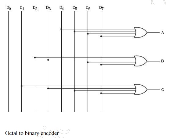
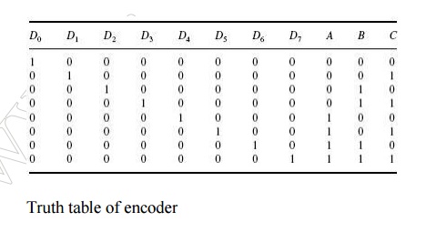
encoder described in
the previous paragraph has an input priority for higher-order digits. Let us
also assume that input lines D2, D4 and D7 are all simultaneously in logic =1‘
state. In that case, only D7 will be encoded and the output will be 111. The
truth table of such a priority Octal to
binary encoder Truth table of encoder encoder will then be modified to what is
shown above in truth table. Looking at the last row of the table, it implies
that, if D7 = 1, then, irrespective of the logic status of other inputs, the
output is 111 as D7 will only be encoded. As another example, Fig. 8.16 shows
the logic symbol and truth table of a 10-line decimal to four-line BCD encoder
providing priority encoding for higher-order digits, with digit 9 having the
highest priority. In the functional table shown, the input line with highest
priority having a LOW on it is encoded irrespective of the logic status of the
other input lines.
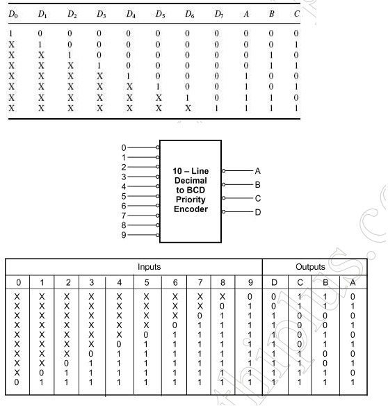
10 line decimal to four line BCD priority encoder
Some of the encoders available in IC form provide
additional inputs and outputs to allow expansion. IC 74148, which is an
eight-line to three -line priority encoder, is an example. ENABLE-IN (EI) and
ENABLE-OUT (EO) terminals on this IC allow expansion. For instance, two 74148s
can be cascaded to build a 16-line to four-line priority encoder.
Magnitude Comparator
A magnitude comparator is a combinational circuit that compares two given numbers and determines whether one is equal to, less than or greater than the other. The output is in the form of three binary variables representing the conditions A = B_A>B and A<B, if A and B are the two numbers being compared. Depending upon the relative magnitude of the two numbers, the relevant output changes state. If the two numbers, let us say, are four-bit binary numbers and are designated as (A3 A2 A1 A0) and (B3 B2 B1 B0), the two numbers will be equal if all pairs of significant digits are equal, that is, A3= B3, A2 = B2, A1= B1 and A0 = B0. In order to determine whether A is greater than or less than B we inspect the relative magnitude of pairs of significant digits, starting from the most significant position. The comparison is done by successively comparing the next adjacent lower pair of digits if the digits of the pair under examination are equal. The comparison continues until a pair of unequal digits is reached. In the pair of unequal digits, if Ai = 1 and Bi = 0, then A > B, and if Ai = 0, Bi= 1 then A < B. If X, Y and Z are three variables respectively representing the A = B, A > B and A < B conditions, then the Boolean expression representing these conditions are given by the equations
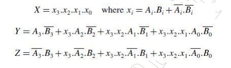
Let us examine equation
(7.25). x3 will be =1‘ only when both A3 and B3 are equal. Similarly,
conditions for x2, x1 and x0 to be =1‘ respectively are equal A2 and B2, equal
A1 and B1 and equal A0 and B0. ANDing of x3, x2, x1 and x0 ensures that X will
be =1‘ when x3, x2, x1 and x0 are in the logic =1‘ state. Thus, X = 1 means
that A = B. On similar lines, it can be visualized that equations (7.26) and
(7.27) respectively represent A > B and A < B conditions. Figure 7.36
shows the logic diagram of a four-bit magnitude comparator.
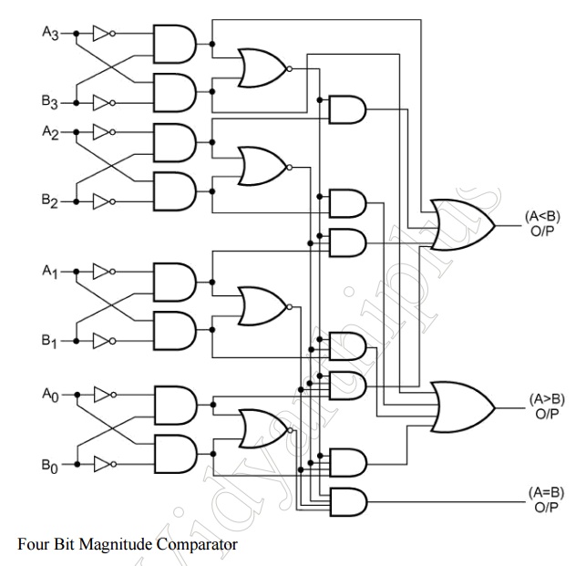
Four Bit Magnitude Comparator
Magnitude comparators are available in IC
form. For example, 7485 is a four-bit magnitude comparator of the TTL logic
family. IC 4585 is a similar device in the CMOS family. 7485 and 4585 have the
same pin connection diagram and functional table. The logic circuit inside
these devices determines whether one four-bit number, binary or BCD, is less
than, equal to or greater than a second four-bit number. It can perform
comparison of straight binary and straight BCD (8-4-2-1) codes. These devices
can be cascaded together to perform operations on larger bit numbers without
the help of any external gates. This is facilitated by three additional inputs
called cascading or expansion inputs available on the IC.
These cascading inputs
are also designated as A = B, A > B and A < B inputs.
Cascading of individual magnitude comparators of the type 7485 or 4585 is discussed in the following paragraphs. IC 74AS885 is another common magnitude comparator. The device is an eight bit magnitude comparator belonging to the advanced Schottky TTL family. It can perform high-speed arithmetic or logic comparisons on two eight-bit binary or 2‘s complement numbers and produces two fully decoded decisions at the output about one number being either greater than or less than the other. More than one of these devices can also be connected in a cascade arrangement to perform comparison of numbers of longer lengths.
Related Topics