Chapter: Electronic Devices : Special Semiconductor Devices
Tunnel diode(Esaki diode)
TUNNEL DIODE (ESA KI DIODE)
·
A tunnel diode or Esaki diode is a type of
semiconductor that is capable of very fast operation, well into the microwave
frequency region, made pos sible by the use of the quantum mechanical effect
called tunneling.
·
It was introduced by Leo Esaki in
1958.Heavily-doped p-n junction. Impurity concentration is 1 part in 10^3 as
compared to 1 part in 10^8 in p-n junction diode. Width of the depletion layer
is very small (about 10 0 A). It is generally made up of Ge and GaAs.
Circuit symbol of tunnel diode
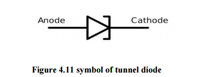
Figure 4.11 symbol of tunnel
diode
Tunneling Phenomenon:
According
to classical mechanics theory, a particle must have an en ergy at least equal
to the the height of a potential-energ y barrier if it has to move from one
side of the barrier to the other. In other words, energy has to be s upplied
from some external source so that th e electrons on N side of junction climb
over the junction barrier to reach the P-side. However if the barrier is thin
such as in tunnel diode ,the Schrodinge r equation(Quantum Mechanics) indicates
that there is a large probability that an electron wil l penetrate through the
barrier. This will hap pen without any loss of energy on the part of electron .
This quantum mechanical behavior is refer red to as tunneling and the
high-impurity P-N junctio n devices are called tunnel-diodes. The tun neling
phenomenon is a majority carrier effect.
1Forward bias operation
Under
normal forward bias operation, as voltage begins to increase, electrons at
first tunnel through the very narrow p–n junction barrier because filled
electron states in the conduction band on the n-side become aligned with empty
valence band hole states on the p-side of the p-n junction. As voltage
increases further t hese states become more misaligned and th e current drops –
this is called negative resistance beca use current decreases with increasing
voltag e. As voltage increases yet further, the diode begins to operate as a
normal diode, where electro ns travel by conduction across the p–n junction,
and no longer by tunneling through the p–n junction barrier. The most important
operating region for a tunnel diode is the negative resistance region.
2Reverse bias operation
When used
in the reverse direction, tunnel diodes are called back diodes (or backward
diodes) and can act as fast rectifiers with zero offset voltage and extreme
linearity for power signals (they have an accurate square law characteristic in
the reverse direction). Under reverse bias, filled states on the p-side become
increasingly aligned with empty states on the n-side and electrons now tunnel
through the pn junction barrier in reverse direction.
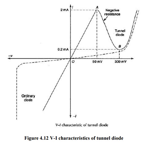
Figure 4.12 V-I characteristics
of tunnel diode
Energy Band Diagram
Energy-band diagram of pn junction in thermal
equilibrium in which both the n and p region are degenerately doped.
At Zero Bias
Simplified
energy-band diagram and I-V characteristics of the tunnel diode at zero bias.
- Zero
current on the I-V diagram;
- All
energy states are filled below EF on both sides of the junction;
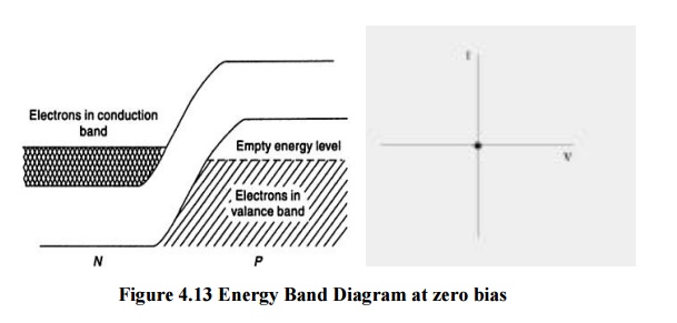
Figure 4.13 Energy Band Diagram
at zero bias
At Small Forward Voltage
Simplified
energy-band diagram and I-V characteristics of the tunnel dio de at a slight
forward bias
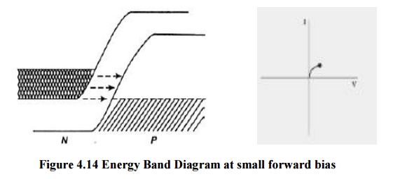
Figure 4.1 4 Energy Band Diagram
at small forward bias
-
Electrons in the conduction band of the n region are directly opposite t o the
empty states in the valence band of the p region.So a finite probability that
some electrons tunnel directly into the empty states resulting in for ward-bias
tunnelling current.
At Maximum Tunnelling Cu rrent
Simplified
energy-band diag ram and I-V characteristics of the tunnel diode at a forward
bias producing maximum tunnelli ng current.The maximum number of electr ons in
the n region are opposite to the maximum number of empty states in the p
region.Hence tunneling current is maximum.
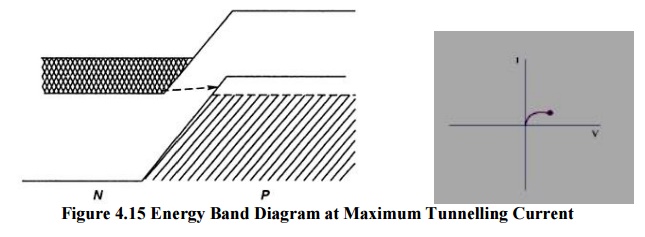
Figure 4.15 Energy Band Diagram at Maximum
Tunnelling Current
Tunnel Diode Equivalent Circuit
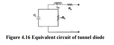
Figure 4.16 Equivalent circuit of
tunnel diode
This is
the equivalent circuit of tunnel diode when biased in negative resistance region.
·
At higher frequency the series R and L can be
ignored.
·
Hence equivalent circuit can be reduced to parallel
combination of junction capacitance and negative resistance.
Applications
·
As logic memory storage device
·
As microwave oscillator
·
In relaxation oscillator circuit
·
As an amplifier
·
As an ultra-high speed switch
Advantages and disadvantages
The tunnel diode is not as widely used these days
as it was oat one time. With the improvement in performance of other forms of
semiconductor technology, they have often become the preferred option.
Nevertheless it is still worth looking at a tunnel diode, considering its
advantages and disadvantages to discover whether it is a viable option.
1 Advantages
·
Very high
speed: The high speed of operation means that the tunnel diode can be used for microwave RF applications.
·
Longevity:
Studies
have been undertaken of the tunnel diode and its performance has been shown to remain stable over long
periods of time, where other semiconductor devices may have degraded.
2 Disadvantages
·
Reproducibility:
It has
not been possible to make the tunnel diode with as reproducible performance to the levels often
needed.
·
Low peak
to valley current ratio: The negative resistance region and the peak to
valley current is not as high as is
often be required to produce the levels of performance that can be attained
with other devices.
One of
the main reasons for the early success of the tunnel diode was its high speed
of operation and the high frequencies it could handle. This resulted from the
fact that while many other devices are slowed down by the presence of minority
carriers, the tunnel diode only uses majority carriers, i.e. holes in an n-type
material and electrons in a p-type material.
The minority
carriers slow down the operation of a device and as a result their speed is
slower. Also the tunnelling effect is inherently very fast.
The
tunnel diode is rarely used these days and this results from its disadvantages.
Firstly they only have a low tunnelling current and this means that they are
low power devices. While this may be acceptable for low noise amplifiers, it is
a significant drawback when they are sued in oscillators as further
amplification is needed and this can only be undertaken by devices that have a
higher power capability, i.e. not tunnel diodes. The third disadvantage is that
they are problems with the reproducibility of the devices resulting in low
yields and therefore higher production costs.
Related Topics