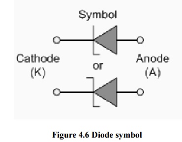
Chapter: Electronic Devices and Circuits : PN Junction Devices
A Zener Diode and its characteristics, Regulator
A ZENER DIODE
A Zener diode is a type of diode that permits current not only in the forward directionlike a normal diode, but also in the reverse direction if the voltage is larger than the breakdownvoltage known as "Zener knee voltage" or "Zener voltage". The device was named after ClarenceZener, who discovered this electrical property.
ü However, the Zener Diode or "Breakdown Diode" as they are sometimes called, arebasically the same as the standard PN junction diode but are specially designed to have a lowpre-determined Reverse Breakdown Voltage that takes advantage of this high reverse voltage.
ü The point at which a zener diode breaks down or conducts is called the "Zener Voltage" (Vz).The Zener diode is like a general-purpose signal diode consisting of a silicon PN junction.
ü When biased in the forward direction it behaves just like a normal signal diode passing the rated current, but when a reverse voltage is applied to it the reverse saturation current remains fairly constant over a wide range of voltages.
ü The reverse voltage increases until the diodes breakdown voltage VB is reached at which point a process called Avalanche Breakdown occurs in the depletion layer and the current flowing through the zener diode increases dramatically to the maximum circuit value (which is usually limited by a series resistor).
ü Thisbreakdown voltage point is called the "zener voltage" for zener diodes.
ü Avalanche Breakdown: There is a limit for the reverse voltage. Reverse voltage can increase until the diode breakdown voltage reaches. This point is called Avalanche Break down region. At this stage maximum current will flow through the zener diode. This breakdown point is referred as ―Zener voltage‖.
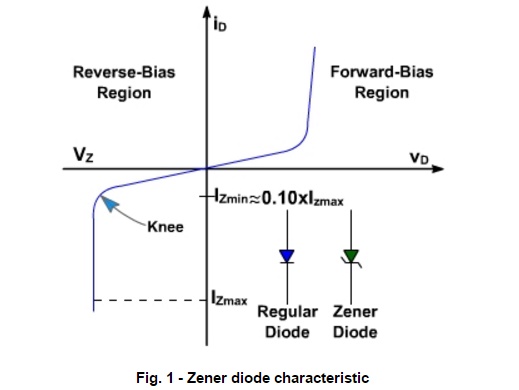
The point at which current flows can be very accurately controlled (to less than 1%tolerance) in the doping stage of the diodes construction giving the diode a specific zener breakdown voltage, (Vz) ranging from a few volts up to a few hundred volts. This zener breakdown voltage on the I-V curve is almost a vertical straight line.
1. Zener diode characteristics
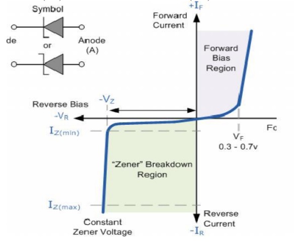
The Zener Diode is used in its "reverse bias" or reverse breakdown mode, i.e. the diodes anode connects to the negative supply. From the I-V characteristics curve above, we can see that the zener diode has a region in its reverse bias characteristics of almost a constant negative voltage regardless of the value of the current flowing through the diode and remains nearly constant even with large changes in current as long as the zener diodes current remains between the breakdown current IZ(min) and the maximum current rating IZ(max).
2. Zener Regulator:
When zener diode is forward biased it works as a diode and drop across it is 0.7 V. When it works in breakdown region the voltage across it is constant (VZ) and the current through diode is decided by the external resistance. Thus, zener diode can be used as a voltage regulator in the configuration shown in figure 2 for regulating the dc voltage. It maintains the output voltage constant even through the current through it changes.
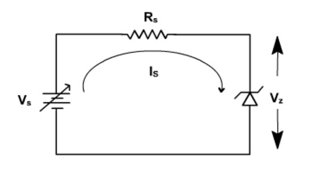
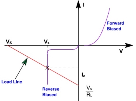
The load line of the circuit is given by Vs= Is Rs + Vz. The load line is plotted along with zener characteristic in figure The intersection point of the load line and the zener characteristic gives the output voltage and zener current.
To operate the zener in breakdown region Vs should always be greater then Vz. Rs is used to limit the current. If the Vs voltage changes, operating point also changes simultaneously but voltage across zener is almost constant. The first approximation of zener diode is a voltage source of Vz magnitude and second approximation includes the resistance also. The two approximate equivalent circuits are shown in below figure
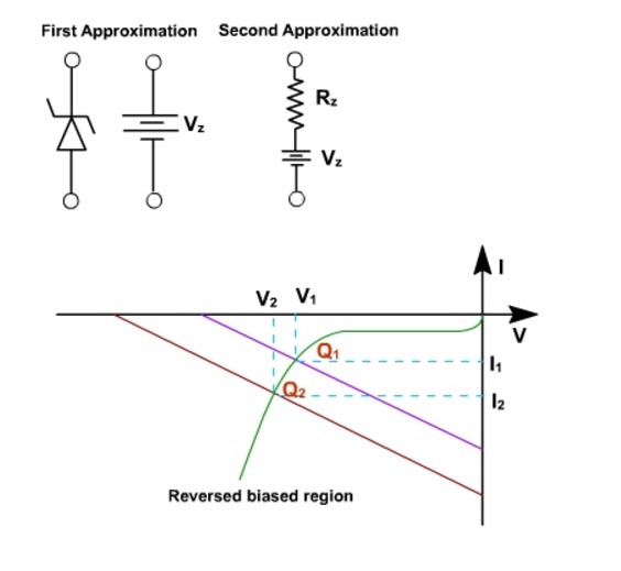
If second approximation of zener diode is considered, the output voltage varies slightly as shown in figure The zener ON state resistance produces more I * R drop as the current increases. As the voltage varies form V1 to V2 the operating point shifts from Q1 to Q2.
The voltage at Q1 is V1 = I1 RZ +VZ and at Q2
V2 = I2 RZ +VZ
Thus, change in voltage is V2 – V1 = ( I2 – I1 ) RZ
Related Topics