Chapter: Solid State Drives : Induction Motor Drives
Voltage source Inverter-driven Induction Motor
Voltage-source Inverter-driven Induction Motor
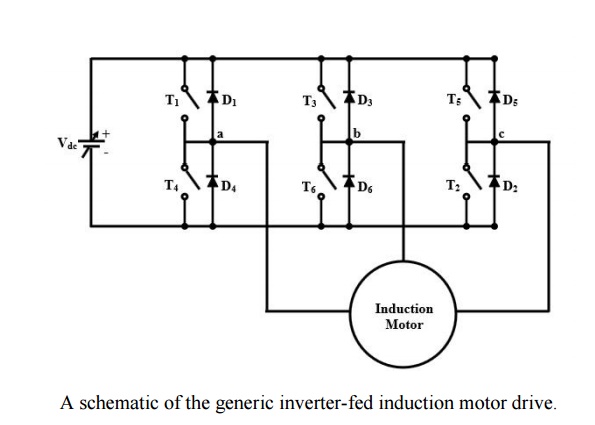
A three-phase variable frequency inverter supplying an induction motor is shown in Figure. The power devices are assumed to be ideal switches. There are two major types of switching schemes for the inverters, namely, square wave switching and PWM switching.
Square wave inverters
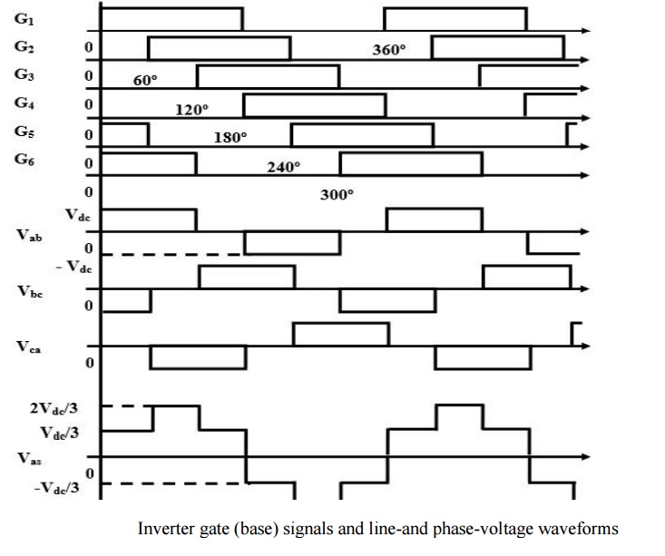
The gating signals and the resulting line voltages for square wave switching are shown in Figure. The phase voltages are derived from the line voltages assuming a balanced three-phase system.
The square wave inverter control is simple and the switching frequency and consequently, switching losses are low. However, significant energies of the lower order harmonics and large distortions in current wave require bulky low-pass filters. Moreover, this scheme can only achieve frequency control. For voltage control a controlled rectifier is needed, which offsets some of the cost advantages of the simple inverter
PWM Principle
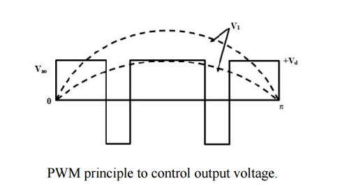
It is possible to control the output voltage and frequency of the PWM inverter simultaneously, as well as optimize the harmonics by performing multiple switching within the inverter major cycle which determines frequency. For example, the fundamental voltage for a square wave has the maximum amplitude (4Vd/π) but by intermediate switching, as shown in Fig. 34.12, the magnitude can be reduced. This determines the principle of simultaneous voltage control by PWM. Different possible strategies for PWM switching exist. They have different harmonic contents. In the following only a sinusoidal PWM is discussed.
Sinusoidal PWM
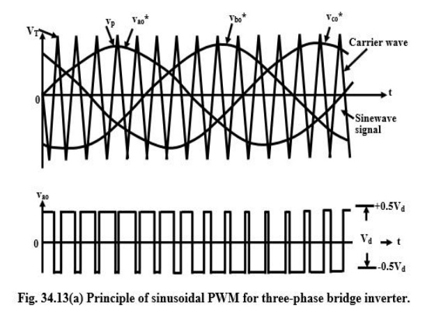
Figure explains the general principle of SPWM, where an isosceles triangle carrier wave of frequency fc is compared with the sinusoidal modulating wave of fundamental frequency f, and the points of intersection determine the switching points of power devices. For example, for phase-a, voltage (Va0) is obtained by switching ON Q1 and Q4 of half -bridge inverter, as shown in the figure . Assuming that f << fc, the pulse widths of va0 wave vary in a sinusoidal manner. Thus, the fundamental frequency is controlled by varying f and its amplitude is proportional to the command modulating voltage. The Fourier analysis of the va0 wave can be shown to be of the form Va0 = 0.5mVd sin(2 Лft+πφ)+ harmonic frequency terms
Where m = modulation index and φ = phase shift of output, depending on the position of the modulating wave. The modulation index m is defined as
m= VP/VT
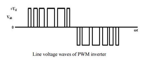
Where Vp = peak value of the modulating wave and VT = peak value of the carrier wave. Ideally, m can be varied between 0 and 1 to give a linear relation between the modulating and output wave. The inverter basically acts as a linear amplifier. The line voltage waveform is shown in Fig.
Current Fed Inverters
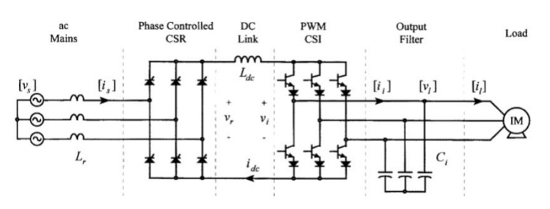
CSI classification is based on the structure of the front-end power converter, which could be either a phase-controlled thyristor rectifier or aPWM current-source rectifier.
A. Phase-Controlled Front-End Rectifiers
These drives use a front-end rectifier based on thyristor-type power switches (Fig. 1), which can be operated with either variable or fixed dc-link current. The performance of the drive converter depends on this last feature.
Variable DC-Link Current Scheme
The CSI is operated with a fixed pattern, which is usually optimized in terms of harmonic spectrum and switching frequency. Thus, the load voltage harmonic distortion is minimum and constant (Table I). However, the dc-link current must be adjusted through transient changes in firing angle to meet the requirements of the load. The dc voltage, on the other hand, is practically constant and independent of the load torque.
This last feature leads to a constant input current displacement factor and, thereby, a constant overall PF. Also, since the dc-link current tracks the output current, the dc-bus and switch conduction losses are kept to a minimum. Usually, the dc-link inductor is designed to have an acceptable current ripple (5%). In order to achieve this value and due to the low-order harmonics produced by the thyristor rectifier (sixth, 12th, etc.), the size of the dc inductor becomes quite bulky. This results in a slow system transient response. Also, the supply current has a high distortion factor % due to the low-order harmonics (fifth, seventh, etc.) injected by the thyristor rectifier. Fig shows typical waveforms of the converter. The rectifier phase angle is only adjusted during transient conditions occurring under load speed and torque variations.
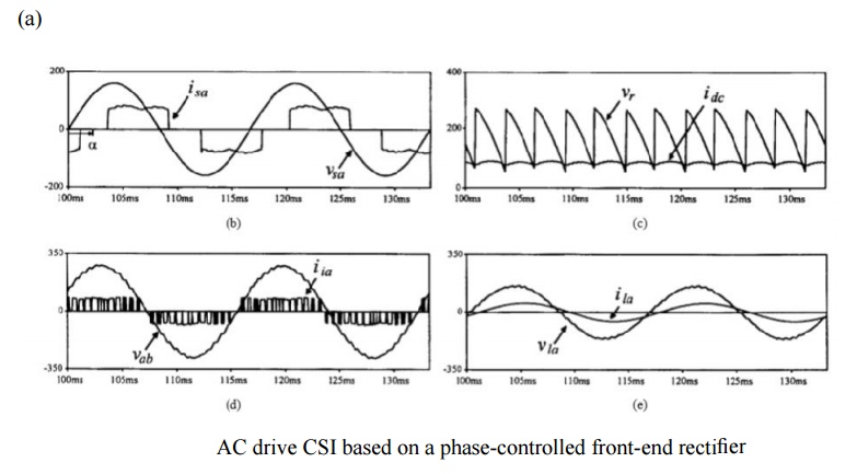
. (a) Power topology. (b) Supply phase voltage and supply line current. (c) DC recti fier voltage and dc-link current. (d) CSI line current and load line voltage. (e) Load phase voltage and load line current.
Fixed DC-Link Current Scheme
Unlike the above control scheme, the CSI is operated with a PWM pattern, which varies as a function of the CSI modulation index. Therefore, the load voltage harmonic distortion is variable and depends upon the speed and load torque (Table I). Since the dc-link current is fixed, the different load power requirements are obtained by varying the dc-link voltage. To achieve this, the input current displacement factor is continuously adjusted and, thereby, the input PF becomes variable and close to zero for light loads. Contrary to the variable dc-link current scheme, the dc -bus and switch conduction losses are always maximum, due to the fact that the dc-link current is always maximum (Table I). Although the dc-link inductor size is as big as the one used in the above scheme, the dynamic response of the load current is improved, due to the variable PWM pattern approach with time responses to modulation index changes of the order of a sampling period. This scheme also presents a high supply current harmonic distortion, due to the thyristor rectifier operation (Table I). Typical waveforms shown in Fig are also applicable in this case; however, in this mode of operation, the rectifier phase angle is continuously adjusted to maintain a constant dc-link current, regardless of the load speed and torque.
B. PWM Front-End Rectifiers
Unlike phase-controlled rectifier topologies, this topology uses a PWM rectifier. This allows a reduction in the harmonics injected into the ac supply. The rectifier is operated with a fixed dc-link current.
Fig. 2 shows typical waveforms of the converter. The PWM pattern is adjusted on a continuous basis to keep a constant dc-link current. In contrast to topologies based on thyristor front-end rectifiers, the overall drive input PF is always greater than 0.95, and the total input current harmonic distortion, which depends on the sampling frequency, is typically lower than 10% (Table I) . Also, since the output inverter is PWM modulated, the system has time responses close to the sampling period. However, the dc-bus losses and switch conduction losses are maximum, since the dc-link current is always equal to its maximum value, regardless of the load speed and torque.
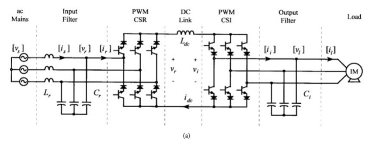
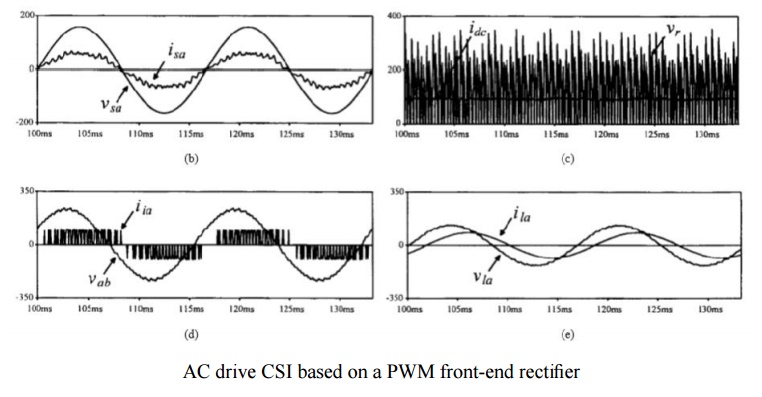
(a) Power topology. (b) Supply phase voltage and supply line current. (c) DC rectifier voltage and dc-link current. (d) CSI line current and load line voltage. (e) Load phase voltage and load line current.
Related Topics