Chapter: Electronic Circuits : Biasing of Discrete BJT and MOSFET
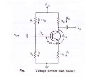
Voltage divider bias circuit
Voltage divider bias circuit:
Figure
shows the voltage divider bias circuit. In this, biasing is provided by three
resistors R1, R2 and RE. The resistors R1&
R2 act as a potential divider giving a fixed voltage to base. If
collector current increases due to change in temperature or change in β,
emitter current IE also increases and voltage drop across RE
increases thus reducing the voltage difference between base and emitter. Due to
reduction in base emitter voltage, base current and collector current reduces.
So we can say that negative feedback exists in emitter bias circuit. This
reduction in collector current compensates for the original change in IC.
Circuit analysis:
Base circuit:
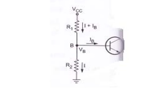
Fig. Base
circuit
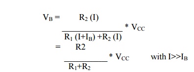
Let us
consider the base circuit as shown in above figure. Voltage across R2
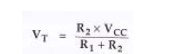
is base voltage VB. Applying voltage divider rule to find VB
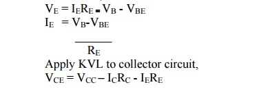
Collector circuit:
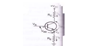
Let us
consider the collector circuit as shown in above figure. Voltage across RE
can be obtained as,
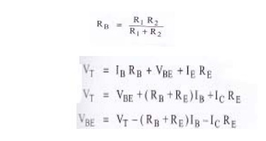
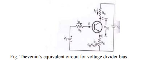
Simplified circuit of voltage divider bias
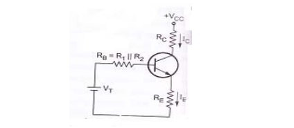
Fig.Thevenin’s
equivalent circuit for voltage divider bias
From
above figure, R1 and R2 are replaced by RB and
VT.
Where RB
is the parallel combination of R=1 and R2
VT
is the thevenin’s voltage
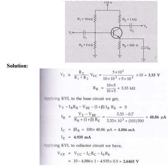
Problem 1:
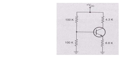
For the given circuit β=100 for silicon transistor. Calculate VCE and IC.
Problem 2:
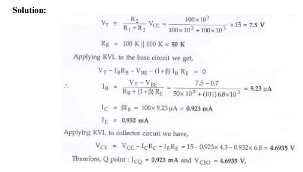
For the given figure find Q point with VCC = 15V, VBE = 0.7V and β = 100.
Stability factor for voltage divider bias:
Stability factor S:
For
determining stability factor S for voltage divider bias, consider the
equivalent circuit. Thevenin’s voltage is given by,
R1,
R2 are replaced by RB which is the parallel combination
of R1 and R2.

Apply KVL
to base circuit,
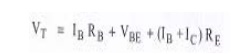
Differentiating
with respect to IC and considering VBE to be independent
of IC,
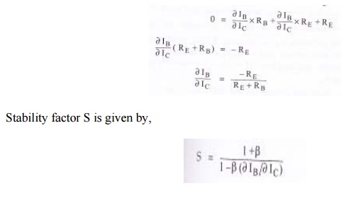
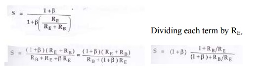
From
above equation, the following points are observed.
1. The
ratio RB /RE controls value of stability factor S. If RB/RE<<
1 then it is reduced to S = (1+β). 1/ (1+β) = 1
Practically
RB/RE not equal to zero. But to have better stability
factor S , we have to keep ratio RB/RE as small as
possible.
2. To keep RB/RE
small, it is necessary to keep RB small. Due to small value of R1
and R2, potential divider circuit will draw more current from VCC
reducing the life of the battery. Another important aspect is that reducing RB
will reduce input impedance of the circuit, since RB comes in
parallel with the input. This reduction of input impedance in amplifier circuit
is not desirable and hence RB cannot be made very small.
3. Emitter
resistance RE is another parameter, it is used to decrease the ratio
RB/RE. Drop across RC will reduce. This shifts
the operating point Q which is not desirable and hence there is limit for
increasing RE.
While
designing voltage divider bias circuit, the following conditions are to be
satisfied,
S – Small
RB - Reasonably small
RE - Not very large
4. If ratio
RB/RE is fixed, S
increases with β. So stability decreases with increasing β.
5. Stability
factor S is essentially independent of β for small value of S.
Substituting
the differentiation value of IB /IC,
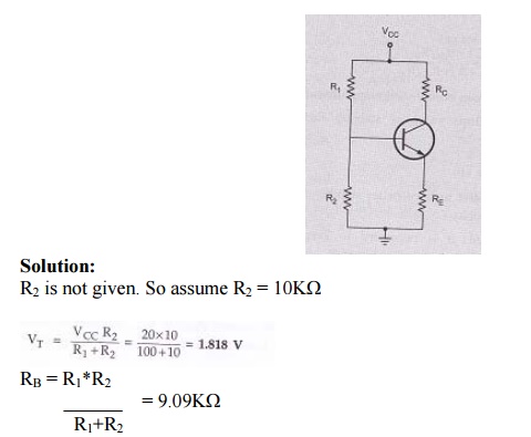
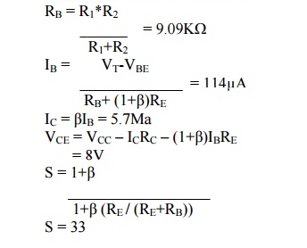
Problem 1:
For the
given circuit, VCC = 20V, RC = 2KΩ, β = 50, VBE
= 0.2V, R1 = 100KΩ, RE = 100Ω. Calculate IB, VCE,
IC and stability factor S.
Related Topics