Chapter: Electronic Devices : Power Devices and Display Devices
V-Groove MOS(VMOS)
V-GROOVE MOS (VMOS)
VMOS Structure
The
structure of VMO S is similar to short-channel power FET t hat is constructed
as a vertical structure. The operation is same as that of a Double-Diffused MO
S (DMOS) device. Take a look at the figure below to know more about the VMOS
structure. This device, like a DMOS device has a channel length which is set by
the difference between the p-typ e and n+ diffusions.
In VMOS,
the p-type epitaxial layer is lightly doped. Along with this, the space
available for the expansion of the depletion region between the p+
diffused layer and the n+ substrate will cause a high breakdown volt
age (BVDS) and a low drain capacitance. That is, the breakdown
voltage will be almost greater t han or equal to 50 Volts. Due to the heavily
doped n+ substrate, the value of the drain series resistance is kept
very small.
The outer
wall of the VMOS has an SiO2 insulation layer, which is covered by
an aluminum layer. This aluminum layer act s as the gate for the device. In a
VMOS dev ice the thickness of the layer does not depend on the mask resolution.
And due to the fact thaat a conventional mask lithographic process is used f or
its fabrication, the p-region is stretched as a channel above the substrate.
Thus, it is easy to make a channel as short as 1micro meter, which is essential
for high-speed MOSFETs.
Another
unique feature of VMOS is the anisotropically-etched V-groove cut normally to
the surface that extends through both the n+, p regions and
penetrates slightly through the epitaxial region. Due to this, it is easier for
the gate to overlay the p-diffusion which acts as the current conducting
channel. The packing density of such devices on a chip is more as the MOSFET’s
are formed on the slopes of the grooves.
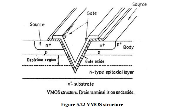
Figure 5.22 VMOS structure
The
V-grooves are produced by an anisotropic or orientation – dependent etching
(ODE) process. The etchant, which is usually KOH at (80 to 100)°C, attacks
silicon very rapidly in the [100] crystallographic direction, but very slowly
in the [111] direction. In the case of (100) oriented silicon substrates the
result will be the production of V-shaped grooves that have (111) side walls as
shown in the figure below.
The angle
of the (111) groove side walls with respect to the (100) silicon surface will
be 54.74°. The width of the opening in the oxide layer controls the width of
the grooves, W. The oxide layer width is used as an etching mask since SiO2
is attacked only very slowly by the etching solution.
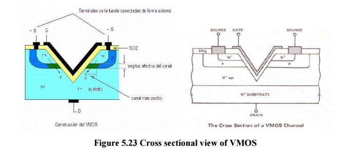
Figure 5.23 Cross sectional view
of VMOS
There is
also the existence of two conduction paths between drain and source, as shown
in Fig., to further contribute to a higher current rating. The net result is a
device with drain currents that can reach the ampere levels with power levels
exceeding 10 W.
Compared with commercially available planar
MOSFETs, VMOS FETs have reduced channel resistance levels and higher current
and power ratings.VMOS FETs have a positive temperature coefficient that will
combat the possibility of thermal runaway.
The
reduced charge storage levels result in faster switching times for VMOS
construction compared to those for conventional planar construction.
In fact, VMOS devices typically have switching
times less than one-half that encountered for the typical BJT transistor.
VMOS Applications
·
Hi-fi audio power amplifiers
·
Broadband high-frequency amplifiers, and
·
Switching power amplifiers which converts ac power sources into dc at arbitrary
voltage.
Such
power supplies made from VMOS will have lower cost, lighter weight, and smaller
size than conventional power supplies.
Related Topics