Chapter: Optical Communication and Networking : Sources and Detectors
The Semiconductor Injection Laser
The Semiconductor Injection Laser
The electroluminescent properties of the forward-biased p–n junction diode have been considered in the preceding sections. Stimulated emission by the recombination of the injected carriers is encouraged in the semiconductor injection laser (also called the injection laser diode (ILD) or simply the injection laser) by the provision of an optical cavity in the crystal structure in order to provide the feedback of photons. This gives the injection laser several major advantages over other semiconductor sources (e.g. LEDs) that may be used for optical communications. These are as follows:
1. High radiance due to the amplifying effect of stimulated emission. Injection lasers will generally supply milliwatts of optical output power.
2. Narrow linewidth on the order of 1 nm (10 Å) or less which is useful in minimizing the effects of material dispersion.
3. Modulation capabilities which at present extend up into the gigahertz range and will undoubtedly be improved upon.
4. Relative temporal coherence which is considered essential to allow heterodyne (coherent) detection in high-capacity systems, but at present is primarily of use in single-mode systems
5. Good spatial coherence which allows the output to be focused by a lens into a spot which has a greater intensity than the dispersed unfocused emission.
This permits efficient coupling of the optical output power into the fiber even for fibers with low numerical aperture. The spatial fold matching to the optical fiber which may be obtained with the laser source is not possible with an incoherent emitter and, consequently, coupling efficiencies are much reduced
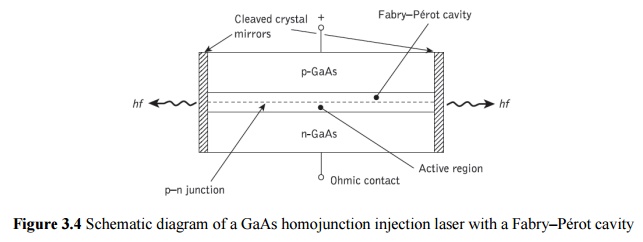
These advantages, together with the compatibility of the injection laser with optical fibers (e.g. size), led to the early developments of the device in the 1960s. Early injection lasers had the form of a Fabry–Pérot cavity often fabricated in gallium arsenide which was the major III–V compound semiconductor with electroluminescent properties at the appropriate wavelength for first-generation systems. The basic structure of this homojunction device is shown in Figure 3.4, where the cleaved ends of the crystal act as partial mirrors in order to encourage stimulated emission in the cavity when electrons are injected into the p-type region. However, as mentioned previously these devices had a high threshold current density (greater than 104 A cm−2) due to their lack of carrier containment and proved inefficient light sources.
High current densities required dictated that these devices when operated at 300 K were largely utilized in a pulsed mode in order to minimize the junction temperature and thus avert damage. Improved carrier containment and thus lower threshold current densities (around 103 A cm−2) were achieved using heterojunction structures.
The DH injection laser fabricated from lattice-matched III–V alloys provided both carrier and optical confinement on both sides of the p–n junction, giving the injection laser a greatly enhanced performance. This enabled these devices with the appropriate heat sinking to be operated in a CW mode at 300 K with obvious advantages for optical communications (e.g. analog transmission). However, in order to provide reliable CW operation of the DH injection laser it was necessary to provide further carrier and optical confinement which led to the introduction of stripe geometry DH laser configurations. Prior to discussion of this structure, however, it is useful to consider the efficiency of the semiconductor injection laser as an optical source.
Stripe geometry
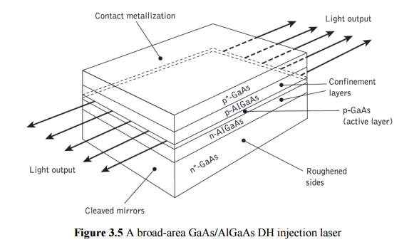
The DH laser structure provides optical confinement in the vertical direction through the refractive index step at the heterojunction interfaces, but lasing takes place across the whole width of the device. This situation is illustrated in Figure 3.5 which shows the broad-area DH laser where the sides of the cavity are simply formed by roughening the edges of the device in order to reduce unwanted emission in these directions and limit the number of horizontal transverse modes. However, the broad emission area creates several problems including difficult heat sinking, lasing from multiple filaments in the relatively wide active area and unsuitable light output geometry for efficient coupling to the cylindrical fibers.
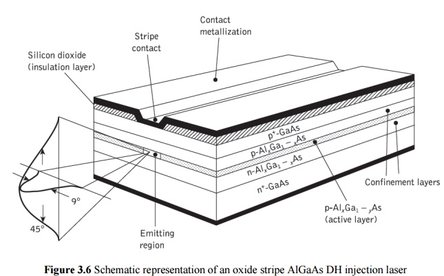
To overcome these problems while also reducing the required threshold current, laser structures in which the active region does not extend to the edges of the device were developed. A common technique involved the introduction of stripe geometry to the structure to provide optical containment in the horizontal plane. The structure of a DH stripe contact laser is shown in Figure 3.6 where the major current flow through the device and hence the active region is within the stripe. Generally, the stripe is formed by the creation of high-resistance areas on either side by techniques such as proton bombardment or oxide isolation.
The stripe therefore acts as a guiding mechanism which overcomes the major problems of the broad-area device. However, although the active area width is reduced the light output is still not particularly well collimated due to isotropic emission from a small active region and diffraction within the structure. The optical output and far-field emission pattern are also illustrated in Figure 6.21. The output beam divergence is typically 45° perpendicular to the plane of the junction and 9° parallel to it. Nevertheless, this is a substantial improvement on the broad-area laser.
Related Topics