Chapter: Embedded Systems Design : Embedded processors
The MC68040
The MC68040
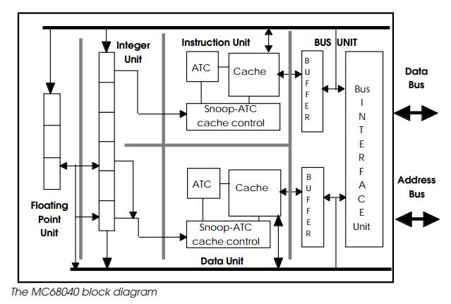
The MC68040 incorporates separate integer and floating point units
giving sustained performances of 20 integer MIPS and 3.5 double precision
Linpack MFLOPS respectively, dual 4 kbyte instruction and data caches, dual
memory management units and an extremely sophisticated bus interface unit. The
block diagram shows how the processor is partitioned into several separate
functional units which can all execute concurrently. It features a full Harvard
architecture internally and is remarkably similar at the block level, to the
PowerPC RISC processor.
The design is revolutionary rather than evolutionary: it takes the ideas
of overlapping instruction execution and pipelining to a new level for CISC
processors. The floating point and integer execution units work in parallel
with the on-chip caches and memory management to increase the overlapping so
that many instructions are executed in a single cycle, and thus give it its
performance.
The pinout reveals a large number of new signals. One major difference
about the MC68040 is its high drive capability. The processor can be configured
on reset to drive either 55 or 5 mA per bus or control pin. This removes the
need for external buffers, reducing chip count and the associated propagation
delays, which often inflict a high speed design. The 32 bit address and 32 bit
data buses are similar to its predecessors although the signals can be
optionally tied together to form a single 32 bit multiplexed data/ address bus.
The User Programmable Attributes (UPA0 and UPA1) are driven according to
2 bits within each page descriptor used by the onboard memory management units.
They are primarily used to enable the MC68040 Bus Snooping protocols, but can
also be used to give additional address bits, software control for external
caches and other such functions. The two size pins, SIZ0 and SIZ1, no longer
indicate the number of remaining bytes left to be transferred as they did on
the MC68020 and MC68030, but are used to generate byte enables for memory
ports. They now indi-cate the size of the current transfer. Dynamic bus sizing
is sup-ported via external hardware if required. Misaligned accesses are
supported by splitting the transfer into a series of aligned accesses of
differing sizes. The transfer type signals, TT1 and TT2, indicate the type of
transfer that is taking place and the Transfer Modifier pins TM0-2 provide
further information. These five pins effec-tively replace the three function
code pins. The TLN0-1 pins indicate the current long word number within a burst
fill access.
The synchronous bus is controlled by the Master and Slave transfer
control signals: Transfer Start (TS*) indicates a valid address on the bus
while the Transfer in Progress (TIP*) signal is asserted during all external
bus cycles and can be used to power up/down external memory to conserve power
in portable appli-cations. These two Master signals are complemented by the
slave signals: Transfer Acknowledge (TA*) successfully terminates the bus
cycle, while Transfer Error Acknowledge (TEA*) terminates the cycle and the
burst fill as a result of an error. If both these signals are asserted on the
first access of the burst, the cycle is terminated and immediately rerun. On
the second, third and fourth accesses, a retry attempt is not allowed and the
processor simply assumes that an error has occurred and will terminate the
burst as normal.
The processor can be configured to use a different signal, Data Latch
Enable DLE to latch read data instead of the rising edge of the BCLK clock. The
internal caches and memory management units can be disabled via the CDIS* and
MDIS* pins respectively.
The programming model
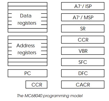
To the programmer the programming model of the MC68040 is the same as
its predecessors such as the MC68030. It has the same eight data and eight
address registers, the vector same base register (VBR), the alternate function
code registers although some codes are reserved, the same dual Supervisor stack
pointer and the two cache control registers although only two bits are now used
to enable or disable either of the two on-chip caches. Inter-nally the
implementation is different. Its instruction execution unit consists of a
six–stage pipeline which sequentially fetches an instruction, decodes it,
calculates the effective address, fetches an address operand, executes the
instruction and finally writes back the results. To prevent pipeline stalling,
an internal Harvard architecture is used to allow simultaneous instruction and
oper-and fetches. It has been optimised for many instructions and addressing
modes so that single-cycle execution can be achieved. The early pipeline stages
are effectively duplicated to allow both paths of a branch instruction to be
processed until the path decision is taken. This removes pipeline stalls and
the subsequent performance degradation. While integer instructions are being
executed, the floating point unit is free to execute floating point
instructions.
Related Topics