Chapter: Microprocessor and Microcontroller : 8086 System Bus Structure
System Bus timings: Minimum mode 8086 system and timings
System Bus timings: Minimum mode 8086 system and
timings
In a
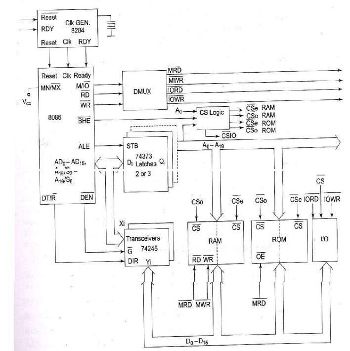
minimum mode 8086 system, the microprocessor 8086 is operated in minimum mode
by strapping its MN/MX* pin to logic1. In this mode, all the control signals
are given out by the microprocessor chip itself. There is a single microprocessor
in the minimum mode system. The remaining components in the system are latches,
transreceivers, clock generator, memory and I/O devices.
The
opcode fetch and read cycles are similar. Hence the timing diagram can be
categorized in two parts, the first is the timing diagram for read cycle and
the second is the timing diagram for write cycle.
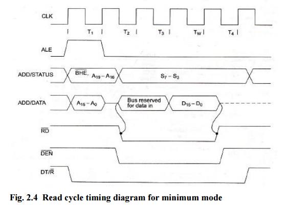
Fig 1.2
shows the read cycle timing diagram. The read cycle begins in T1 with the
assertion of the address latch enable (ALE) signal and also M/IO* signal.
During the negative going edge of this signal, the valid address is latched on
the local bus. The BHE* and A0 signals address low, high or both bytes. From Tl
to T4, the M/IO* signal indicates a memory or I/O operation. At T2 the address
is removed from the local bus and is sent to the output. The bus is then
tristated. The read (RD*) control signal is also activated in T2 .The read (RD)
signal causes the addressed device to enable its data bus drivers. After RD*
goes low, the valid data is available on the data bus. The addressed device
will drive the READY line high, when the processor returns the read signal to
high level, the addressed device will again tristate its bus drivers.
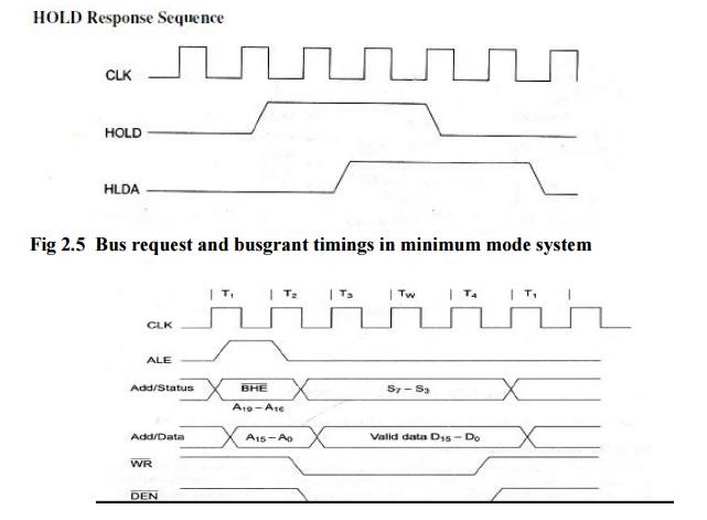
A write
cycle also begins with the assertion of ALE and the emission of the address.
The M/IO* signal is again asserted to indicate a memory or I/O operation. In T2
after sending the address in Tl the processor sends the data to be written to
the addressed location. The data remains on the bus until middle of T4 state.
The WR* becomes active at the beginning ofT2 (unlike RD* is somewhat delayed in
T2 to provide time for floating). The BHE* and A0 signals are used to select
the proper byte or bytes of memory or I/O word to be read or written. The
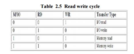
M/IO*, RD* and WR* signals indicate the types of data transfer as specified in
Table
Table 2.5 Read write cycle
Related Topics