Chapter: Digital Principles and System Design : Synchronous Sequential Logic
Synchronous Sequential Logic
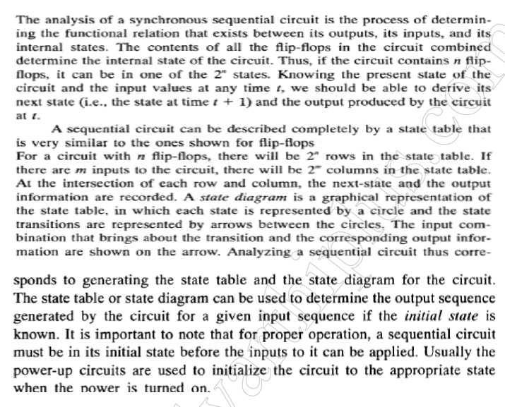
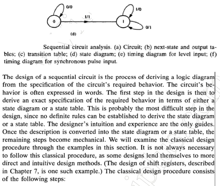
SYNCHRONOUS SEQUENTIAL LOGIC
SEQUENTIAL LOGIC DESIGN
1 Flip Flops and their conversion
The flip-flop is an important element of such circuits. It has the interesting property of memory: It can be set to a state which is retained until explicitly reset.
R-S Flip-Flop
A flip-flop, as stated earlier, is a bistable circuit. Both of its output states are stable. The circuit remains in a particular output state indefinitely until something is done to change that output status. Referring to the bistable multivibrator circuit discussed earlier, these two states were those of the output transistor in saturation (representing a LOW output) and in cut-off (representing a HIGH output). If the LOW and HIGH outputs are respectively regarded as =0‘ and =1‘, then the output can either be a =0‘ or a =1‘. Since either a =0‘ or a =1‘ can be held indefinitely until the circuit is appropriately triggered to go to the other state, the circuit is said to have memory. It is capable of storing one binary digit or one bit of digital information. Also, if we recall the functioning of the bistable multivibrator circuit, we find that, when one of the transistors was in saturation, the other was in cut-off. This implies that, if we had taken outputs from the collectors of both transistors, then the two outputs would be complementary.
In the flip-flops of various types that are available in IC form, we will see that all these devices offer complementary outputs usually designated as Q and Q‘ The R-S flip-flop is the most basic of all flip-flops. The letters =R‘ and =S‘ here stand for RESET and SET. When the flip-flop is SET, its Q output goes to a =1‘ state, and when it is RESET it goes to a =0‘ state. The Q‘ output is the complement of the Q output at all times.
J-K Flip-Flop
A J-K flip-flop behaves in the same fashion as an R-S flip-flop except for one of the entries in the function table. In the case of an R-S flip-flop, the input combination S = R = 1 (in the case of a flip-flop with active HIGH inputs) and the input combination S = R = 0 (in the case of a flip-flop with active LOW inputs) are prohibited. In the case of a J-K flip-flop with active HIGH inputs, the output of the flip-flop toggles, that is, it goes to the other state, for J = K = 1 . The output toggles for J = K = 0 in the case of the flip-flop having active LOW inputs. Thus, a J-K flip-flop overcomes the problem of a forbidden input combination of the R-S flip-flop. Figures below respectively show the circuit symbol of level-triggered J-K flip-flops with active HIGH and active LOW inputs, along with their function tables.
The characteristic tables for a J-K flip-flop with active HIGH J and K inputs and a J-K flip-flop with active LOW J and K inputs are respectively shown in Figs 10.28(a) and (b)_ The corresponding Karnaugh maps are shown in Fig below for the characteristics table of Fig and in below for the characteristic table below. The characteristic equations for the Karnaugh maps of below figure is shown next
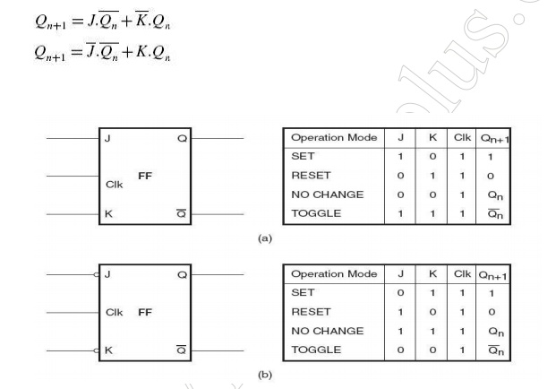
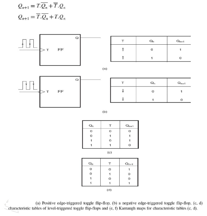
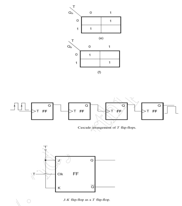
FIG a. JK flip flop with active high inputs, b. JK flip flop with active low inputs Toggle Flip-Flop (T Flip-Flop) The output of a toggle flip-flop, also called a T flip-flop, changes state every time it is triggered at its T input, called the toggle input. That is, the output becomes =1‘ if it was =0‘ and =0‘ if it was =1‘. Positive edge-triggered and negative edge-triggered T flip-flops, along with their function tables. If we consider the T input as active when HIGH, the characteristic table of such a flip-flop is shown in Fig. If the T input were active when LOW, then the characteristic table would be as shown in Fig. The Karnaugh maps for the characteristic tables of Figs shown respectively. The characteristic equations as written from the Karnaugh maps are as follows:
J-K Flip-Flop as a Toggle Flip-Flop
If we recall the function table of a J-K flip-flop, we will see that, when both J and K inputs of the flip-flop are tied to their active level (=1‘ level if J and K are active when HIGH, and =0‘ level when J and K are active when LOW), the flip-flop behaves like a toggle flip-flop, with its clock input serving as the T input. In fact, the J-K flip-flop can be used to construct any other flip-flop. That is why it is also sometimes referred to as a universal flip-flop. Figure shows the use of a J-K flip-flop as a T flip-flop.
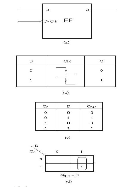
D Flip-Flop
A D flip-flop, also called a delay flip-flop, can be used to provide temporary storage of one bit of information. Figure shows the circuit symbol and function table of a negative edge-triggered D flip-flop. When the clock is active, the data bit (0 or 1) present at the D input is transferred to the output. In the D flip-flop of Fig the data transfer from D input to Q output occurs on the negative-going (HIGH-to-LOW) transition of the clock input. The D input can acquire new status
D Type Flip Flop
J-K Flip-Flop as D Flip-Flop
Figure below shows how a J-K flip-flop can be used as a D flip-flop. When the D input is a logic =1‘, the J and K inputs are a logic =1‘ and =0‘ respectively.
According to the function table of the J-K flip-flop, under these input conditions, the Q output will go to the logic =1‘ state when clocked. Also, when the D input is a logic =0‘, the J and K inputs are a logic =0‘ and =1‘ respectively.
Again, according to the function table of the J-K flip-flop, under these input conditions, the Q output will go to the logic =0‘ state when clocked. Thus, in both cases, the D input is passed on to the output when the flip-flop is clocked.
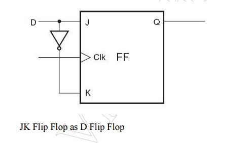
JK Flip Flop as D Flip Flop
Analysis and Synthesis of Synchronous Sequential Circuit Design of synchronous sequential circuit
Related Topics