Chapter: Digital Electronics : Synchronous and Asynchronous Sequential Circuits
Shift Registers
SHIFT REGISTERS
1. Introduction
Shift registers are a type of sequential logic circuit, mainly for storage of digital data. They are a group of flip-flops connected in a chain so that the output from one flip-flop becomes the input of the next flip-flop. Most of the registers possess no characteristic internal sequence of states. All the flip-flops are driven by a common clock, and all are set or reset simultaneously.
The basic types of shift registers are such as Serial In - Serial Out, Serial In - Parallel Out, Parallel In - Serial Out, Parallel In - Parallel Out, and bidirectional shift registers.
2. Serial In - Serial Out Shift Registers
A basic four-bit shift register can be constructed using four D flip-flops, as shown below. The operation of the circuit is as follows. The register is first cleared, forcing all four outputs to zero. The input data is then applied sequentially to the D input of the first flip-flop on the left (FF0). During each clock pulse, one bit is transmitted from left to right. Assume a data word to be 1001. The least significant bit of the data has to be shifted through the register from FF0 to FF3.
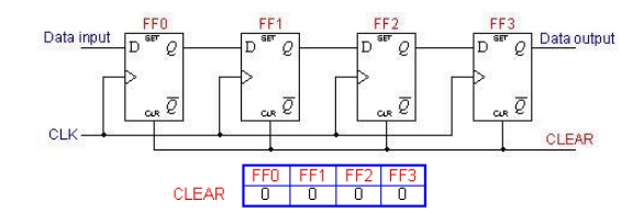
In order to get the data out of the register, they must be shifted out serially. This can be done destructively or non-destructively. For destructive readout, the original data is lost and at the end of the read cycle, all flip-flops are reset to zero.
To avoid the loss of data, an arrangement for a non-destructive reading can be done by adding two AND gates, an OR gate and an inverter to the system. The construction of this circuit is shown below.
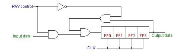
The data is loaded to the register when the control line is HIGH (ie WRITE). The data can be shifted out of the register when the control line is LOW (ie READ).
3. Serial In - Parallel Out Shift Registers
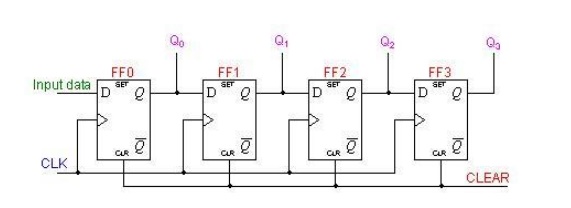
For this kind of register, data bits are entered serially in the same manner as discussed in the last section. The difference is the way in which the data bits are taken out of the register. Once the data are stored, each bit appears on its respective output line, and all bits are available simultaneously. A construction of a four-bit serial in - parallel out register is shown below.
4. Parallel In - Serial Out Shift Registers
A four-bit parallel in - serial out shift register is shown below. The circuit uses D flip-flops and NAND gates for entering data (ie writing) to the register.
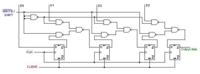
D0, D1, D2 and D3 are the parallel inputs, where D0 is the most significant bit and D3 is the least significant bit. To write data in, the mode control line is taken to LOW and the data is clocked in. The data can be shifted when the mode control line is HIGH as SHIFT is active high. The register performs right shift operation on the application of a clock pulse.
5. Parallel In - Parallel Out Shift Registers
For parallel in - parallel out shift registers, all data bits appear on the parallel outputs immediately following the simultaneous entry of the data bits. The following circuit is a four-bit parallel in - parallel out shift register constructed by D flip-flops.
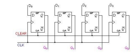
The D's are the parallel inputs and the Q's are the parallel outputs. Once the register is clocked, all the data at the D inputs appear at the corresponding Q outputs simultaneously.
Related Topics