Chapter: Digital Principles and System Design : Synchronous Sequential Logic
Shift Register
SHIFT REGISTER
Register:
A set of
n flip-flops.
Each
flip-flop stores one bit.
Two basic functions: data storage and data movement
Shift
Register:
A
register that allows each of the flip-flops to pass the stored information to
its adjacent neighbor.
A shift register is a cascade of Flip flops, sharing
the same clock, which has the output of any one but the last flip-flop
connected to the "data" input of the next one in the chain, resulting
in a circuit that shifts by one position the one- dimensional "bit array" stored in
it, shifting in the data present at its
input and shifting out the last bit in
the array, when enabled to do so by a transition of the clock input. More generally, a shift register may
be multidimensional, such that its
"data in" input and stage
outputs are themselves bit arrays: this is implemented simply by running several shift registers of
the same bit-length in parallel.
Types of shift register
Shift registers can have a
combination of serial and parallel inputs and outputs, including serial-in,
parallel-out (SIPO) and parallel-in, serial-out (PISO) types. There are also
types that have both serial and parallel input and types with serial and
parallel output. There are also bi-directional shift registers which allow you
to vary the direction of the shift register. The serial input and outputs of a
register can also be connected together to create a circular shift register.
One could also create multi-dimensional shift registers, which can perform more
complex computation.
ü Serial-in, serial-out
Destructive readout- These are
the simplest kind of shift register. The data string is presented at 'Data In',
and is shifted right one stage each time 'Data Advance' is brought high. At
each advance, the bit on the far left (i.e. 'Data In') is shifted into the
first flip-flop's output. The bit on the far right (i.e. 'Data Out') is shifted
out and lost.The data are stored after each flip-flop on the 'Q' output, so
there are four storage 'slots' available in this arrangement, hence it is a
4-Bit Register. To give an idea of the shifting pattern, imagine that the
register holds 0000 (so all storage slots are empty).
As 'Data In' presents
1,1,0,1,0,0,0,0 (in that order, with a pulse at 'Data Advance' each time. This
is called clocking or strobing) to the register, this is the result. The left
hand column corresponds to the left-most flip-flop's output pin, and so on.So
the serial output of the entire register is 11010000 (). As you can see if we
were to continue to input data, we would get exactly what was put in, but
offset by four 'Data Advance' cycles. This arrangement is the hardware
equivalent of a queue. Also, at any time, the whole register can be set to zero
by bringing the reset (R) pins high. This arrangement performs destructive
readout -each datum is lost once it been shifted out of the right-most bit.
Non-destructive readout- Non-destructive
readout can be achieved using the configuration shown below. Another
input line is added - the Read/Write Control. When this is high (i.e. write)
then the shift register behaves as normal, advancing the input data one place
for every clock cycle, and data can be lost from the end of the register.
However, when the R/W control is set low (i.e. read), any data shifted out of
the register at the right becomes the next input at the left, and is kept in
the system. Therefore, as long as the R/W control is set low, no data can be
lost from the system.
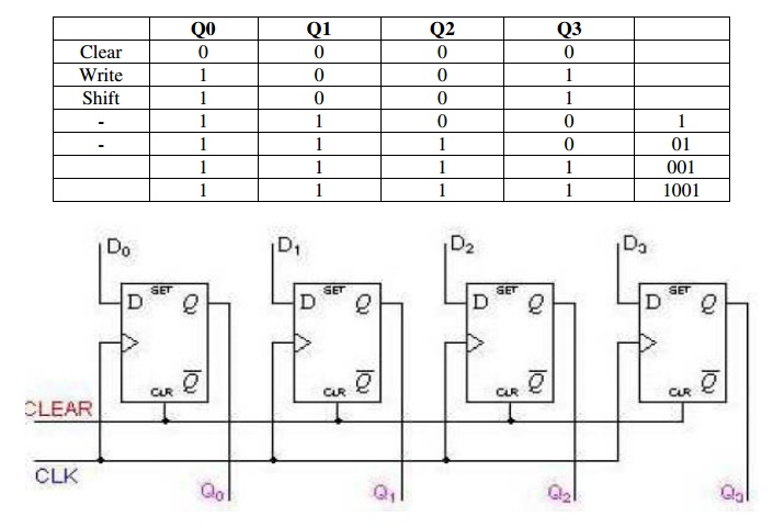
Example: Basic four-bit shift register
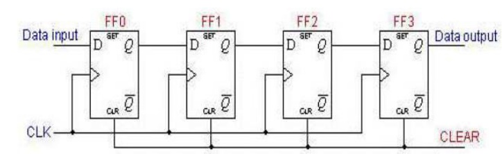
The operation of the circuit is as follows,
·
The register is first cleared, forcing all four
outputs to zero.
·
The input data is then applied sequentially to the
D input of the first flip-flop on the left (FF0).
·
During each clock pulse, one bit is transmitted
from left to right. Assume a data word to be 1001.
·
The least significant bit of the data has to be
shifted through the register from FF0 to FF3.
In order to get the data out of the register, they must be
shifted out serially. This can be done destructively or non-destructively. For
destructive readout, the original data is lost and at the end of the read
cycle, all flip-flops are reset to zero.
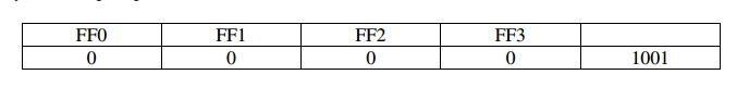
The data is loaded to the register when the control line is
HIGH (ie WRITE). The data can be shifted out of the register when the control
line is LOW (ie READ).
ü Serial-in, parallel-out
This configuration allows conversion from serial to parallel
format. Data are input serially, as described in the SISO section above. Once
the data has been input, it may be either read off at each output
simultaneously, or it can be shifted out and replaced.
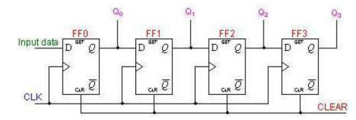
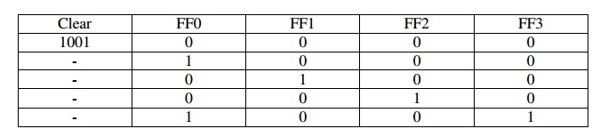
In the table below, we can see how the four-bit binary number
1001 is shifted to the Q outputs of the register.
ü Parallel-in, serial-out
This configuration has the data
input on lines D1 through D4 in parallel format. To write the data to the
register, the Write/Shift control line must be held LOW. To shift the data, the
W/S control line is brought HIGH and the registers are clocked. The arrangement
now acts as a SISO shift register, with D1 as the Data Input. However, as long
as the number of clock cycles is not more than the length of the data-string,
the Data Output, Q, will be the parallel data read off in order.
Example: A four-bit parallel in - serial
out shift register is shown below. The circuit uses D flip -flops and
NAND gates for entering data (ie writing) to the register.
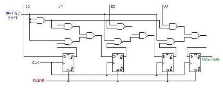
D0, D1, D2 and D3 are the
parallel inputs, where D0 is the most significant bit and D3 is the least
significant bit. To write data in, the mode control line is taken to LOW and
the data is clocked in. The data
can be shifted when the mode
control line is HIGH as SHIFT is active high. The register performs right shift
operation on the application of a clock pulse, as shown in the table below.
ü Parallel-in, parallel-out
This configuration allows
conversion from parallel to parallel format. Data input are in parallel, as
described in the PISO section above. Once the data has been input, it may be
either read off at each output simultaneously, or it can be shifted out and
replaced.
The D's are the parallel inputs
and the Q's are the parallel outputs. Once the register is clocked, all the
data at the D inputs appear at the corresponding Q outputs simultaneously
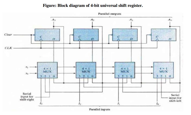
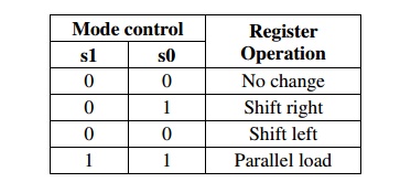
ü Universal shift register
A register capable of shifting in one direction only is a
unidirectional shift register .One that can shift in both directions is a
bidirectional shift register. If the register has both shifts and
parallel-loads, it is referred as universal shift register. The circuit
consists of four D flip-flops and four multiplexers. The four multiplexers have
two common selection inputs s1 and s0.
Figure: Block diagram of 4-bit universal shift
register.
Applications of shift registers
Shift registers can be found in
many applications. Here is a list of a few. 1. To produce time delay
The serial in -serial out shift
register can be used as a time delay device. The amount of delay can be
controlled by:
1. The
number of stages in the register
2. The clock
frequency
3. To
convert serial data to parallel data
4. To
simplify combinational logic.
Related Topics