Chapter: Electronic Devices : Semiconductor Diode
Semiconductor Diode
SEMICONDUCTOR DIODE
SEMICONDUCTOR
A semiconductor is a material which has electrical
conductivity to a degree between that of a metal (such as copper) and that of
an insulator (such as glass). Semiconductors are the foundation of modern
electronics, including transistors, solar cells, light -emitting diodes (LEDs),
quantum dots and digital and analog integrated circuits.
DIODE
Diode –
Di + ode
Di means two and ode means electrode. So physical
contact of two electrodes is known as diode and its important function is
alternative current to direct current.
REVIEW OF INTRINSIC AND EXTRINSIC
SEMICONDUCTORS
1 INTRINSIC SEMICONDUCTOR
An intrinsic semiconductor is one, which is pure
enough that impurities do not appreciably affect its electrical behaviour. In
this case, all carriers are created due to thermally or optically excited
electrons from the full valence band into the empty conduction band. Thus equal
numbers of electrons and holes are present in an intrinsic semiconductor.
Electrons and holes flow in opposite directions in an electric field, though
they contribute to current in the same direction since they are oppositely
charged. Hole current and electron current are not necessarily equal in an
intrinsic semiconductor, however, because electrons and holes have different
effective masses (crystalline analogues to free inertial masses).
The concentration of carriers is strongly dependent
on the temperature. At low temperatures, the valence band is completely full
making the material an insulator. Increasing the temperature leads to an
increase in the number of carriers and a corresponding increase in
conductivity. This characteristic shown by intrinsic semiconductor is different
from the behaviour of most metals, which tend to become less conductive at
higher temperatures due to increased phonon scattering.
Both silicon and germanium are tetravalent, i.e.
each has four electrons (valence electrons) in their outermost shell. Both
elements crystallize with a diamond-like structure, i.e. in such a way that
each atom in the crystal is inside a tetrahedron formed by the four atoms which
are closest to it. Each atom shares its four valence electrons with its four
immediate neighbours, so that each atom is involved in four covalent bonds.
2 EXTRINSIC SEMICONDUCTOR
An
extrinsic semiconductor is one that has been doped with impurities to modify
the number and type of free charge carriers. An extrinsic semiconductor is a
semiconductor that has been doped,
that is, into which a doping agent has been introduced, giving it different
electrical properties than the intrinsic (pure) semiconductor.
Doping involves adding doping atoms to an intrinsic
semiconductor, which changes the electron and hole carrier concentrations of
the semiconductor at thermal equilibrium. Dominant carrier concentrations in an
extrinsic semiconductor classify it as either an n-type or p-type
semiconductor.
A pure or intrinsic conductor has thermally
generated holes and electrons. However these are relatively few in number. An enormous
increase in the number of charge carriers can by achieved by introducing
impurities into the semiconductor in a controlled manner. The result is the
formation of an extrinsic semiconductor. This process is referred to as doping.
There are basically two types of impurities: donor impurities and acceptor
impurities. Donor impurities are made up of atoms (arsenic for example) which
have five valence electrons. Acceptor impurities are made up of atoms (gallium
for example) which have three valence electrons.
The two
types of extrinsic semiconductor are
1 N-TYPE SEMICONDUCTORS
Extrinsic semiconductors with a larger electron
concentration than hole concentration are known as n-type semiconductors. The
phrase 'n-type' comes from the negative charge of the electron. In n-type
semiconductors, electrons are the majority carriers and holes are the minority
carriers. N-type semiconductors are created by doping an intrinsic
semiconductor with donor impurities.
In an n-type semiconductor, the Fermi energy level
is greater than that of the intrinsic semiconductor and lies closer to the
conduction band than the valence band. Arsenic has 5 valence electrons, however,
only 4 of them form part of covalent bonds. The 5th electron is then free to
take part in conduction. The electrons are said to be the majority carriers and
the holes are said to be the minority carriers.
2 P-TYPE SEMICONDUCTORS
As opposed to n-type semiconductors, p-type
semiconductors have a larger hole concentration than electron concentration.
The phrase 'p-type' refers to the positive charge of the hole. In p-type
semiconductors, holes are the majority carriers and electrons are the minority
carriers. P-type semiconductors are created by doping an intrinsic
semiconductor with acceptor impurities. P-type semiconductors have Fermi energy
levels below the intrinsic Fermi energy level.
The Fermi energy level lies closer to the valence
band than the conduction band in a p-type semiconductor. Gallium has 3 valence
electrons, however, there are 4 covalent bonds to fill.
The 4th
bond therefore remains vacant producing a hole. The holes are said to be the
majority carriers and the electrons are said to be the minority carriers.
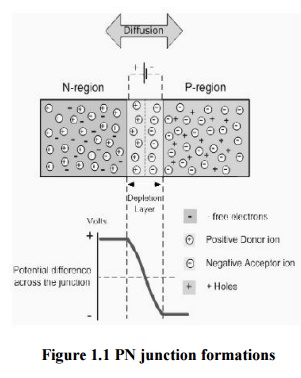
PN JUNCTION
When the
N and P-type semiconductor materials are first joined together a very large
density gradient exists between both sides of the junction so some of the free
electrons from the donor impurity atoms begin to migrate across this newly
formed junction to fill up the holes in the P-type material producing negative
ions.
However, because the electrons have moved across the junc tion from the
N-type silicon to the P-type silicon, they leave behind positively charged do
nor ions (ND) on the negative side and now the holes from the acceptor impurity
migrate across the junction in the opposite direction into the reg ion are
there are large numbers of free electr ons.
As a result, the charge density of the P-type along
the junction i s filled with negatively charged acceptor ions (NA), and the
charge density of the N-type along the junction becomes positive. This charge
transfer of electrons and holes across the junction is k nown as diffusion.
This process continues back and forth until the
number of electro ns which have crossed the junction have a large en ough
electrical charge to repel or prevent any more carriers from crossing the
junction.
The regions on both sides of the junction become
depleted of any free carriers in comparison to the N and P type materials away
from the junction. Eventually a state of equilibrium (electrically neutral
situation) will occur producing a "potential barrier" zone around the
area of the junction as the donor atoms repel the holes and the acceptor atoms
repel the electrons. Since no free charge carriers can rest in a position where
there is a potential barrier the regions on both sides of the junction become
depleted of any more free carriers in comparison to the N and P type materials
away from the junction. This a rea around the junction is now called the
Depletion L ayer.
THE PN JUNCTION
The total charge on each side of the junction must
be equal and opposite to maintain a neutral charge condition around the
junction.
If the depletion layer region has a distance D, it
therefore must therefore penetrate into the silicon by a distance of D p for
the positive side, and a distance of D n for the negative side giving a
relationship between the two of Dp.NA = Dn.ND in order to maintain charge
neutrality also called equilibrium.
PN JUNCTION DISTANCE
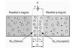
Figure 1.2 PN junction distance under built in potential E0
As the
N-type material has lost electrons and the P-type has lost holes, the N-type
material has become positive with respect to the P-type. Then the presence of
impurity ions on both sides of the junction cause an electric field to be e
stablished across t his region with the N- side at a positive voltage relative
to the P-side.
The
problem now is that a free charge requires some extra energy to overcome the
barrier that now exists for it to be able to cross the depletion region junct
ion. This electric field created by the diffu sion process has created a
"built-in po tential difference" across the junction with an
open-circuit (zero bias) potential of:
Where: E 0
is the zero bias junction voltage, VT the thermal voltage of 26mV at
room temperature,
ND and NA are th e impurity concentrations and
ni is
the intrinsic c oncentration.
A
suitable positive voltage (forward bias) applied between the two ends of the PN
junction can supply the free electrons and holes with the extra en ergy. The
external voltage required to overcome this potential barrier that now exists is
very much dependent upon the type of semiconduc tor material used and its
actual temperature. Typically at room temperature the voltage acro ss the
depletion layer for silicon is about 0 .6 - 0.7 volts and for germanium is
about 0.3 - 0.35 volts. This potential barrier will always exist even if the
device is not connected to an y external power source.
The significance of t his built-in potential across
the junction is th at it opposes both the flow of holes and elect rons across
the junction and is why it is c alled the potential barrier. In practice, a PN
j unction is formed within a single crystal of material rather than just simply
joining or fusing together two separate pieces. Electrical contacts are also
fused onto either side o f the crystal to enable an electrical connect ion to
be made to an external circuit. Then th e resulting device that has been made
is cal led a PN junction Diode or Signal Diode.
DEPLETION LAYER PN JUNCTION
If one side of crystal pure semiconductor Si(silicon) or Ge(Germ anium)
is doped with acceptor impurity atoms and the other side is doped with donor
impurity atoms , a PN junction is formed as shown in figure. P region has high
concentration of holes a nd N region contains large number of electrons.
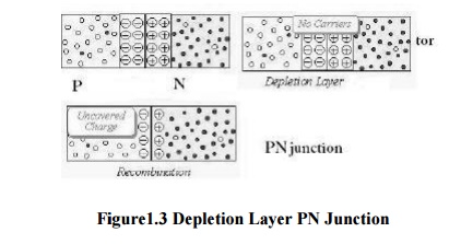
Figure1.3 Depletion Layer PN
Junction
As soon as the junction is formed, free electrons
and holes cross through the junction by the process of diffusion. During this
process, the electrons crossing the junction from N-region into P-region ,
recombine with holes in the P-region very close to the junction. Similarly
holes crossing the junction fr om the P-region into the N-region, recombine
with electrons in the N- region very close to the junction. Thus a region is
formed, whic h does not have any mobile charge very close to th e junction.
This region is called the depletion layer of PN junction.
In this region, on th e left side of the junction, the acceptor at oms
become negative ions and on the right side of the junction, the donor atoms
become positive ions as shown in figure.
FUNCTION OF DEPL ETION LAYER OF
PN JUNCTION
An electric field is set up, between the donor and acceptor ions in the
depletion layer of the pn junction .The potenti al at the N-side is higher than
the potential at P-side. Therefore electrons in the N- side are prevented to go
to the lower potential of P -side. Similarly, holes in the P-side find
themselves at a lower potential and are prevented to cro ss to the N-side.
Thus, there is a barrier at the ju nction which opposes the movement of the
majority charge carriers.
The difference of potential from one side of the barrier to the other
side of the barrier is called potential barrier. Th e potential barrier is
approximately 0.7V for a silicon PN junction and 0.3V for germanium PN
junction. The distance from one side of th e barrier to the other side is
called the width of the barrier, which depends on the nature of the material.
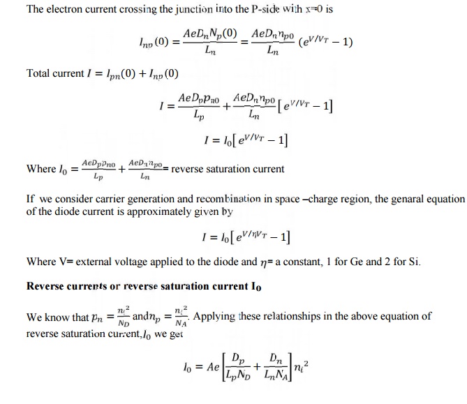
QUANTITATIVE THEORY OF P-N DIODE
CURRENTS
To derive
the expressio n for the total current as function of applie d voltage (neglect
the barrier width)When diode is fo rward biased, holes injected from the p to n
material. The concentration pn of holes in the n-side is increased above
equilibrium value pno is the diffusion
length for holes
in the N-material
and the injected
or excess concentration at x=0 is
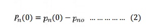
Equation
(2) shows the exponential decrease of density pn(x) with distance x into the
N-material.
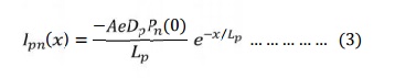
From
equation 3 hole current decreases exponentially with distance. It is depending
on Pn(0) , because it is a function of applied voltage. Ipn depends on applied
voltage or injected concentration is a function of voltage.
Law of Junction
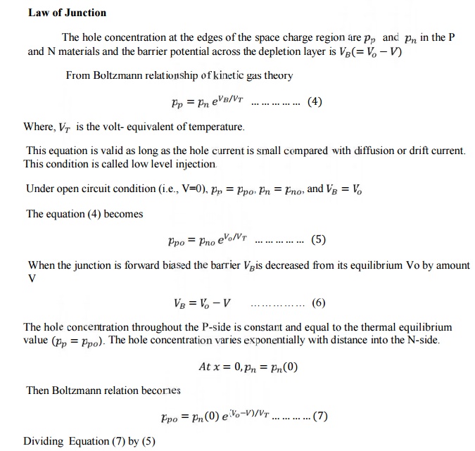
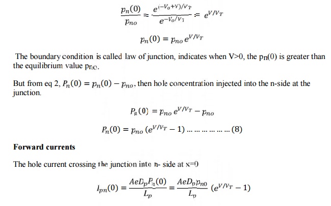
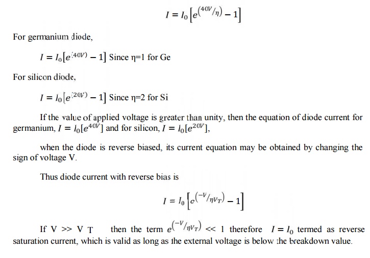
1 DIODE CURRENT EQUATION
The diode
current equation relating the voltage V and current I is given by
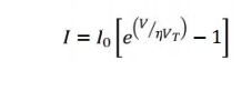
where
I – diode
current
Io –
diode reverse saturation current at room temperature
V –
External voltage applied to the diode
η - a
constant, 1 for Ge and 2 for Si VT = kT/q = T/11600, thermal voltage
K –
Boltzmann‘s constant (1.38066x10^-23 J/K) q – Charge of electron (1.6x10^-19 C)
T –
Temperature of the diode junction
At room
temperature (T=300 K), VT = 26mV. Substituting this value in current equation,
DRIFT AND DIFFUSION CURRENTS
·
The flow of charge (ie) current through a
semiconductor material are of two types namely drift & diffusion. (ie) The
net current that flows through a (PN junction diode) semiconductor material has
two components
(i) Drift
current (ii) Diffusion current
1 DRIFT CURRENT
· When an electric field is applied across the
semiconductor material, the charge carriers attain a certain drift velocity Vd
, which is equal to the product of the mobility of the charge carriers and the
applied Electric Field intensity E .
Drift
velocity Vd = mobility of the charge carriers X Applied Electric field
intensity.
· Holes move towards the negative terminal of
the battery and electrons move towards the positive terminal of the battery.
This combined effect of movement of the charge carriers constitutes a current
known as ― the drift current.
· Thus the drift current is defined as the flow
of electric current due to the motion of the charge carriers under the
influence of an external electric field.
· Drift current due to the
charge carriers such as free electrons and holes are the current passing
through a square centimeter perpendicular to the direction of flow.
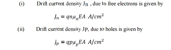
Where, n -
Number of free electrons per cubic centimetre.
P - Number of holes per cubic centimetre
μ(n) – Mobility of electrons in cm2 / Vs
μ (p) – Mobility of holes in cm2 / Vs
E –
Applied Electric filed Intensity in V /cm
q –
Charge of an electron = 1.6 x 10⁻¹⁹
coulomb.
2 DIFFUSION CURRENT
· It is
possible for an electric current to flow in a semiconductor even in the absence
of the applied voltage provided a concentration gradient exists in the
material.
· A
concentration gradient exists if the number of either elements or holes is
greater in one region of a semiconductor as compared to the rest of the Region.
Figure
1.4 (a) Exess hole concentration varying along the axis in an N-type
semiconductor bar, (b) The resulting diffusion current
→ In a semiconductor material the change carriers
have the tendency to move from the region of higher concentration to that of
lower concentration of the same type of charge carriers.
Thus the movement of charge carriers takes place
resulting in a current called diffusion current.
As indicated in fig a, the hole concentration p(x)
in semiconductor bar varies from a high value to a low value along the x-axis
and is constant in the y and z directions.
Diffusion current density due to holes Jp is given by
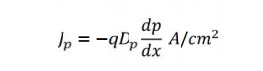
Since the hole density p(x) decreases with
increasing x as shown in fig b, dp/dx is
negative and the minus sign in
equation is needed in order that Jp has positive sign in the positive x
direction.
Diffusion current density due to the free electrons
is given by
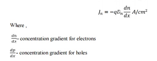
Dn and Dp
– diffusion coefficient for electrons and holes
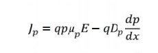
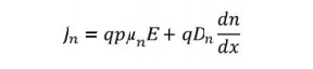
Total Current
The total current in a semiconductor is the sum of
both drift and diffusion currents that is given by
FORWARD BIAS CONDITION
When
positive terminal of the battery is connected to the P-type and negative
terminal to N-type of the PN junction diode that is known as forward bias
condition.
Operation
The applied potential in external battery acts in opposition to the
internal potential barrier which disturbs the equilibrium.
As soon as equilibrium is disturbed by the
application of an external voltage, the Fermi level is no longer continuous
across the junction.
Under the forward bias condition the applied positive
potential repels the holes in P type region so that the holes move towards the
junction and the applied positive potential repels the electrons in N type
region so that the electrons move towards the junction.
When the applied potential is more than the
internal barrier potential the depletion region and internal potential barrier
disappear.
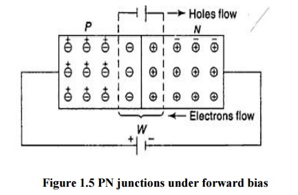
Figure 1.5 PN junctions under
forward bias
V-I Characteristics
As the forward voltage increased for VF < Vo,
the forward current IF almost zero because the potential barrier prevents the
holes from P region and electrons from N region to flow across the depletion
region in opposite direction.
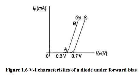
Figure 1.6 V-I characteristics of
a diode under forward bias
For VF > Vo, the potential barrier at the
junction completely disappears and hence, the holes cross the junction from P
to N type and electrons cross the junction to opposite direction, resulting
large current flow in external circuit.
A feature noted here is the cut in voltage or
threshold voltage VF below which the current is very small.At this voltage the
potential barrier is overcome and the current through the junction starts to
increase rapidly.
Cut in
voltage is 0.3V for germanium and 0.7 for silicon.
UNDER REVERSE BIAS CONDITION
When the negative terminal of the battery is
connected to the P-type and positive terminal to N-type of the PN junction
diode that is known as forward bias condition.
Operation
The holes
from the majority carriers of the P side move towards the negative terminal of
the battery and electrons which from the majority carrier of the N side are
attracted towards the positive terminal of the battery.
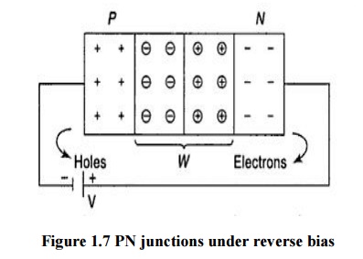
Figure 1.7 PN junctions under
reverse bias
Hence, the width of the depletion region which is
depleted of mobile charge carriers increases. Thus, the electric field produced
by applied reverse bias, is in the same direction as the electric field of the
potential barrier.
Hence the resultant potential barrier is increased
which prevents the flow of majority carriers in both directions. The depletion
width W is proportional to under reverse bias.
V-I characteristics
Theoretically
no current flow in the external circuit. But in practice a very small amount of
current of the order of few microamperes flows under reverse bias.
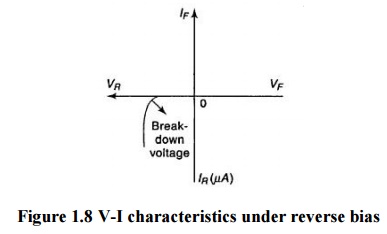
Figure 1.8 V-I characteristics
under reverse bias
Electrons forming covalent bonds of semiconductor atoms in the P and N
type regions may absorb sufficient energy from heat and light to cause breaking
covalent bonds. So electron hole pairs continuously produced.
Consequently
the minority carriers electrons in the P region and holes in the N region,
wander over to the junction and flow towards their majority carrier side giving
rise a small reverse current. This current is known as reverse saturation
current Io.
The magnitude of this current is depends on the
temperature because minority carr ier is thermally broken covalent bonds.
DIODE CHARACTERISTICS
1. Maximum Forward Current
The Maximum Forward Current (IF(max)) is as its
name implies the maximum forward current allowed to flow through the device.
When the diode is conducting in the forward bias condition, it has a very small
"ON" resistance across the PN junction and therefore, power is
dissipated across this junction (Ohm´s Law) in the form of heat. Then,
exceeding its (IF(max)) value will cause more heat to be generated across the
junction and the diode will fail due to thermal overload, usually with
destructive consequences. When operating diodes around their maximum current
ratings it is always best to provide additional cooling to dissipate the heat
produced by the diode.
For example, our small 1N4148 signal diode has a maximum current rating
of about 150mA with a power dissipation of 500mW at 25oC. Then a resistor must
be used in series with the diode to limit the forward current, (IF(max))
through it to below this value.
2. Peak Inverse Voltage
The Peak Inverse Voltage (PIV) or Maximum Reverse
Voltage (VR(max)), is the maximum allowable Reverse operating voltage that can
be applied across the diode without reverse breakdown and damage occurring to
the device. This rating therefore, is usually less than the "avalanche breakdown"
level on the reverse bias characteristic curve. Typical values of VR(max) range
from a few volts to thousands of volts and must be considered when replacing a
diode.The peak inverse voltage is an important parameter and is mainly used for
rectifying diodes in AC rectifier circuits with reference to the amplitude of
the voltage were the sinusoidal waveform changes from a positive to a negative
value on each and every cycle.
3. Forward Power Dissipation
Signal diodes have a Forward Power Dissipation,
(PD(max)) rating. This rating is the maximum possible power dissipation of the
diode when it is forward biased (conducting). When current flows through the
signal diode the biasing of the PN junction is not perfect and offers some
resistance to the flow of current resulting in power being dissipated (lost) in
the diode in the form of heat. As small signal diodes are nonlinear devices the
resistance of the PN junction is not constant, it is a dynamic property then we
cannot use Ohms Law to define the power in terms of current and resistance or
voltage and resistance as we can for resistors. Then to find the power that
will be dissipated by the diode we must multiply the voltage drop across it
times the current flowing through it: PD = VxI
4. Maximum Operating Temperature
The
Maximum Operating Temperature actually relates to the Junction Temperature (TJ)
of the diode and is related to maximum power dissipation. It is the maximum
temperature allowable before the structure of the diode deteriorates and is
expressed in units of degrees centigrade per Watt, ( oC/W ). This value is
linked closely to the maximum forward current of the device so that at this
value the temperature of the junction is not exceeded. However, the maximum
forward current will also depend upon the ambient temperature in which the
device is operating so the maximum forward current is usually quoted for two or
more ambient temperature values such as 25oC or 70oC.
SWITCHING CHARACTERISTICS
Diodes are often used in switching mode. When the applied bias voltage
to the PN diode is suddenly reversed in opposite direction and it reaches a
steady state at a interval of time that is called the recovery time.
Forward recovery time is defined is the time
required the forward voltage or current to reach a specified value after
switching diode from its reverse to forward biased state.
When PN diode is forward biased the minority
electrons concentration in P region is linear. If the junction is suddenly
reversed at t1 then because of stored electronic charge, the reverse current IR
is initially of the same magnitude as forward current IF.
The diode will continue to conduct until the
injected or excess minority carrier density (p-po) or (n-no) has dropped to
zero shown in fig. c.
In fig. b the applied voltage Vi = VF for the time up to t1 is in the
direction to forward bias the diode. The resistance RL is large so that the
drop across RL is large when compared to the drop across diode. Then the
current is I= VF / RL = IF.
At time t=t1 the input voltage is reversed to the value of –VR current
does not become zero and the value is I= VR / RL = IR shown in fig d..
During the time interval from t1 to t2 the injected minority carriers
have remained stored and hence this interval is called the storage time (t1).
After the instant t=t2, the diode gradually recovers and ultimately
reaches the steady state. The time interval between t2 and instant t3 when the
diode has recovered nominally is called the transition time tt.
The recovery said to have completed (i) when even the minority carriers
remote from the junction have difference to the junction and crossed it. (ii)
when the junction transition capacitance C across the reverse biased junction
has got charged through the external resistor RL to the voltage –VR.
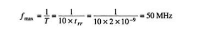
For
commercial switching type diodes the reverse recovery time trr ranges from less
than 1ns up to as high as 1us. In order to minimize the effect of reverse
current the time period of the operating frequency should be a minimum of approximately
10 times trr.
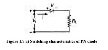
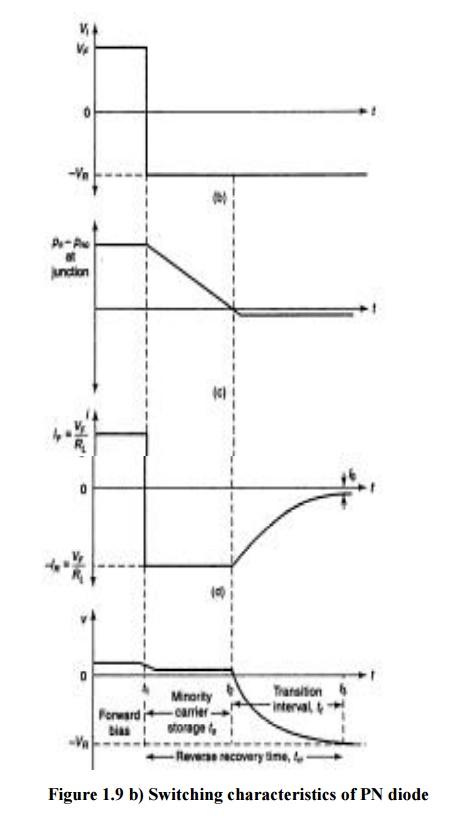
Figure 1.9 b) Switching
characteristics of PN diode
For
example if diode has trr of 2ns its operating frequency is
The reverse recovery time can be reduced b
shortening the length of the P region in a PN junction diode.
The stored storage and switching time can be
reduced by introduction of gold impurities into junction diode by diffusion.
The gold doping also called a life time killer, increases the recombination
rate and removes the stored minority carriers.This technique is used to produce
diodes and other active devices for high speed applications.
APPLICATION OF PN DIODE
·
Can be used as rectifier in DC Power Supplies.
·
In Demodulation or Detector Circuits.
·
In clamping networks used as DC Restorers
·
In clipping circuits used for waveform generation.
·
As switches in digital logic circuits.
·
In demodulation circuits.
Related Topics